Unit 4 - Notes
Unit 4: Introduction to HDLs in Digital Systems
1. Hardware Description Languages (HDL)
History and Evolution
Hardware Description Languages (HDLs) are specialized computer languages used to describe the structure and behavior of electronic circuits, particularly digital logic circuits.
- Early Days (1970s): Logic design was primarily done via schematic capture (drawing gates). As complexity grew, this became unmanageable.
- The 1980s (The Birth of HDLs):
- Verilog: Created by Phil Moorby at Gateway Design Automation (1984) for simulation. It was proprietary until made open in 1990 (OVI) and IEEE standardized in 1995 (IEEE 1364).
- VHDL (VHSIC HDL): Commissioned by the US Department of Defense in 1981. Standardized by IEEE in 1987. It was designed for documentation and verification.
- Modern Era:
- SystemVerilog: An extension of Verilog that includes object-oriented programming features for advanced verification (IEEE 1800).
- High-Level Synthesis (HLS): Using C/C++ to generate HDL.
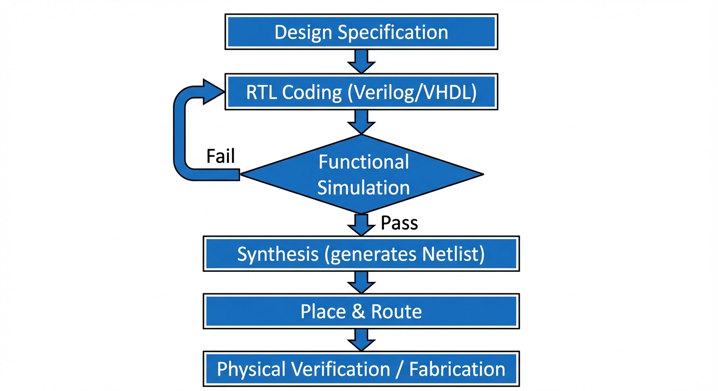
Typical HDL-based Design Flow
The transition from a concept to a physical chip involves several critical stages.
- Design Specification: Defining the functionality, timing, and area constraints.
- RTL Design (Coding): Writing the code in Verilog/VHDL at the Register Transfer Level.
- Simulation (Functional Verification): Testing the logic using a testbench to ensure the code behaves as expected without timing delays.
- Synthesis: Converting the RTL code into a gate-level netlist (AND, OR, NOT gates, Flip-Flops) mapped to a specific technology library.
- Place and Route: Arranging the gates on the physical silicon die and wiring them.
- Timing Verification: Ensuring signals arrive on time (Setup and Hold time checks).
Comparison: HDL vs. Software Programming Languages
| Feature | Software Languages (C, Python, Java) | Hardware Description Languages (Verilog, VHDL) |
|---|---|---|
| Execution Model | Sequential: Instructions execute one line after another. | Parallel/Concurrent: Multiple blocks of hardware operate simultaneously. |
| Target | Runs on a CPU/Processor. | Describes the hardware structure (ASIC/FPGA). |
| Time Concept | No inherent concept of simulation time (only clock cycles of the CPU). | Precise control over timing, propagation delays, and clock edges. |
| Variables | Memory locations holding values. | Wires (connections) and Registers (storage elements). |
Verilog Overview
Verilog is syntactically similar to C but structurally different.
Key Components:
- Module: The basic building block.
- Ports: Inputs and outputs (pins).
- Wire: A physical connection (combinational logic).
- Reg: A variable that holds a value (sequential logic).
Example Code (D Flip-Flop):
module d_flip_flop (
    input clk,
    input reset,
    input d,
    output reg q
);
    // Trigger on rising edge of clock or rising edge of reset
    always @(posedge clk or posedge reset) begin
        if (reset)
            q <= 1'b0;  // Non-blocking assignment
        else
            q <= d;
    end
endmodule
2. Register Transfer and Micro Operations
Register Transfer Language (RTL)
RTL is a symbolic notation used to describe the micro-operations transfers between registers.
- Registers: Denoted by capital letters (e.g., for Memory Address Register, for Program Counter).
- Transfer: Denoted by a replacement operator ().
- : Transfer content of R1 to R2.
- Control Functions: Boolean conditions that determine when a transfer occurs.
- Interpretation: If signal , then load the content of into at the next clock pulse.
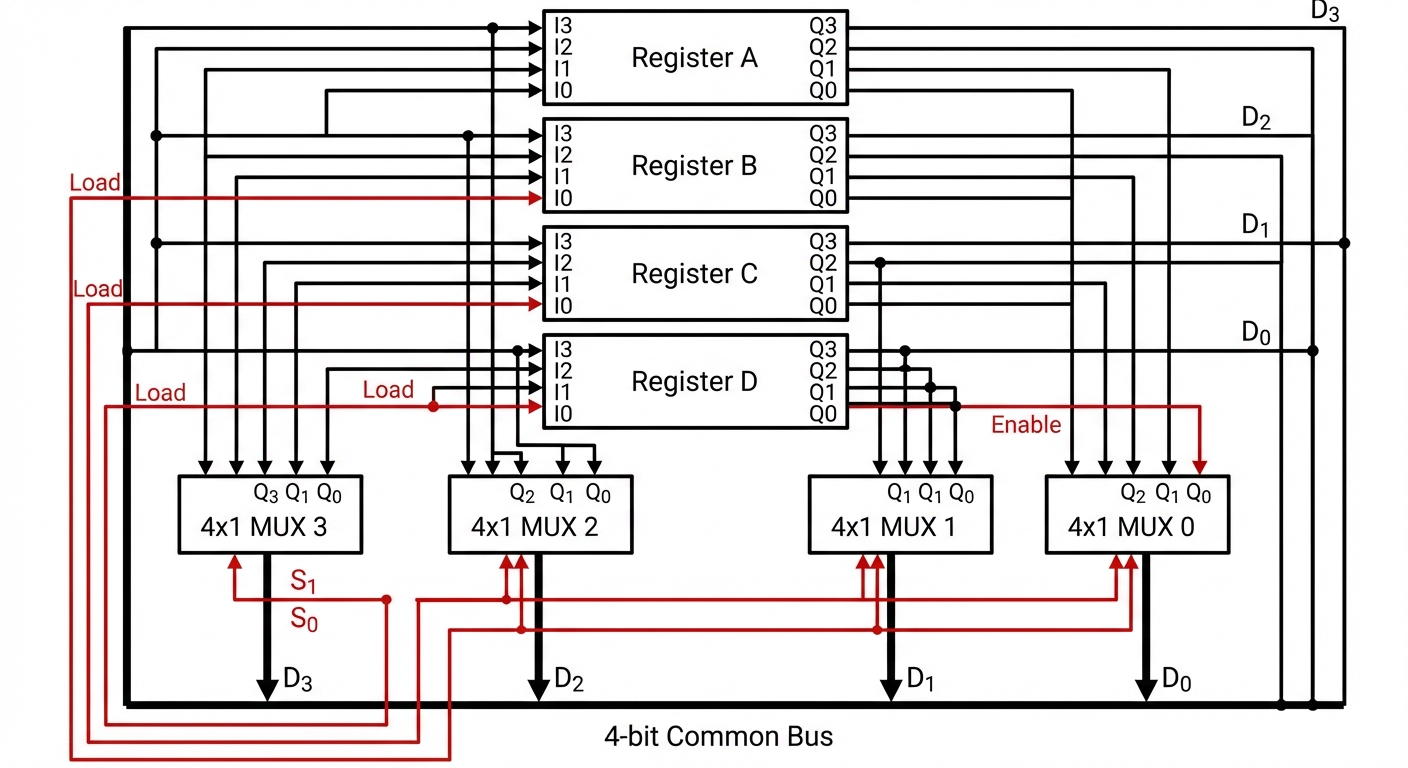
Bus and Memory Transfer
The Bus System:
In a digital system with many registers, connecting wires between all of them is impractical. A Common Bus is used to create a shared communication path.
- Multiplexer-based Bus: Uses MUXes to select which register puts data onto the bus.
- Three-State Bus: Uses Tri-state buffers (High Impedance state) to control access to the bus line.
Memory Transfer:
- Read Operation: Transfer data from memory word () at address () to Data Register ().
- Write Operation: Transfer data from Data Register () to memory at address ().
3. Micro Operations
Micro operations are the atomic operations executed on data stored in registers during one clock pulse.
Types of Micro Operations
- Register Transfer Micro operations: Transfer binary information from one register to another.
- Arithmetic Micro operations: Perform numeric arithmetic on data.
- Logic Micro operations: Perform bit manipulation.
- Shift Micro operations: Shift data in registers.
Detailed Operations
1. Arithmetic Micro operations:
- Addition:
- Subtraction: (Using 2's complement).
- Increment:
- Decrement:
2. Logic Micro operations:
These operate on individual bits of the registers (bitwise).
- XOR: (Used to clear registers or complement bits).
- AND: Masking (forcing 0s).
- OR: Setting bits (forcing 1s).
3. Shift Micro operations & Shift Registers:
A Shift Register is a cascade of flip-flops sharing the same clock, where the output of each flip-flop is connected to the "data" input of the next.
- Logical Shift: Transfers 0 through the serial input.
- Logical Shift Left (shl): Multiplies by 2.
- Logical Shift Right (shr): Divides by 2 (unsigned).
- Arithmetic Shift: Used for signed numbers.
- Arithmetic Shift Right (ashr): Preserves the sign bit (MSB).
- Circular Shift (Rotate): Circulates bits without loss. The MSB moves to LSB (or vice versa).
4. Computer Arithmetic Algorithms
Addition and Subtraction
- Binary Adder: Constructed using Full Adders in a cascade (Ripple Carry Adder).
- Binary Subtractor: Implemented using a binary adder by taking the 2's complement of the subtrahend (B) and adding it to the minuend (A).
Multiplication Algorithm (Hardware Implementation)
Multiplication is repeated addition and shifting.
Basic Sequence:
- Check the Least Significant Bit (LSB) of the Multiplier.
- If LSB = 1, add Multiplicand to the partial product.
- Shift the Multiplicand left (or partial product right).
- Repeat for all bits.
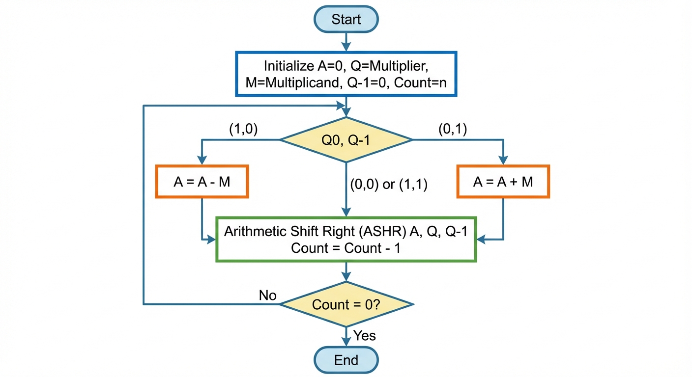
Booth Multiplication Algorithm
Booth's algorithm is a technique used for signed binary multiplication (using 2's complement notation). It treats positive and negative numbers uniformly.
Concept:
It operates on the principle that a string of 1s in the multiplier (e.g., 00111100) can be treated as .
- It looks at two bits at a time: The current bit of the multiplier () and the previous bit ().
The Rules:
Let be the accumulator (initially 0), be the Multiplier, and be the Multiplicand. is an extra bit initially set to 0.
| (Current LSB) | (Previous Bit) | Operation |
|---|---|---|
| 0 | 0 | Arithmetic Shift Right (ASHR) |
| 1 | 1 | Arithmetic Shift Right (ASHR) |
| 0 | 1 | ; then ASHR |
| 1 | 0 | ; then ASHR |
Example of Booth Algorithm:
Multiply (using 4-bit registers).
- (7)
- (3)
- (2's complement of 7)
| Cycle | Step | A | Q | Action | |
|---|---|---|---|---|---|
| Init | 0000 | 0011 | 0 | ||
| 1 | Check | 0000 | 0011 | 0 | Subtract M () |
| 1001 | 0011 | 0 | |||
| ASHR | 1100 | 1001 | 1 | ||
| 2 | Check | 1100 | 1001 | 1 | Shift only |
| ASHR | 1110 | 0100 | 1 | ||
| 3 | Check | 1110 | 0100 | 1 | Add M () |
| 0101 | 0100 | 1 | ( carry ignored) | ||
| ASHR | 0010 | 1010 | 0 | ||
| 4 | Check | 0010 | 1010 | 0 | Shift only |
| ASHR | 0001 | 0101 | 0 | Result: 00010101 (21) |