Unit 5 - Notes
Unit 5: Solid State Physics
1. Free Electron Theory
1.1 Introduction
The free electron theory attempts to explain the physical properties of metals, such as electrical and thermal conductivity.
- Classical Free Electron Theory (Drude-Lorentz Model): Assumes metals contain a gas of free electrons that move randomly inside the lattice. These electrons collide with positive ion cores, but between collisions, they move freely.
- Quantum Free Electron Theory (Sommerfeld Model): Improves upon the classical model by treating electrons as quantum particles obeying Fermi-Dirac statistics and the Pauli Exclusion Principle. Electrons are confined to a potential well, and energy levels are quantized.
1.2 Drift and Diffusion Current (Qualitative)
Current in solids arises from two distinct transport mechanisms:
A. Drift Current
- Definition: The directed flow of charge carriers under the influence of an applied external electric field.
- Mechanism: When an electric field () is applied, carriers accelerate but undergo collisions. This results in a constant average velocity called drift velocity ().
- Formula:
- where is current density, is conductivity, is carrier concentration, is charge, and is mobility.
B. Diffusion Current
- Definition: The flow of charge carriers from a region of higher concentration to a region of lower concentration.
- Mechanism: This is a statistical process driven by the random thermal motion of particles seeking equilibrium (concentration gradient). No electric field is required.
- Formula (Fick's Law):
- where is the diffusion coefficient and is the concentration gradient.
2. Statistical Mechanics of Electrons
2.1 Fermi Energy ()
Fermi energy is a critical concept in quantum mechanics referring to the energy state of electrons in a solid.
- Definition at 0K: The highest energy level occupied by an electron in a solid at absolute zero temperature (0 Kelvin).
- Significance: It separates filled energy states from empty energy states at 0K. Only electrons near the Fermi level participate in conduction at temperatures above 0K.
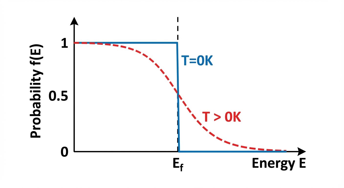
2.2 Fermi-Dirac Distribution Function
This function gives the probability that a quantum state with energy is occupied by an electron at a given temperature .
The Formula:
Where:
- = Boltzmann constant
- = Absolute temperature
- = Fermi Energy
Behavior with Temperature:
- At :
- If , the exponential term is $0$, so (100% occupancy).
- If , the exponential term is , so (0% occupancy).
- Result: A step function.
- At :
- Electrons near the Fermi level gain thermal energy and jump to higher states. The step function "smears" out.
- At exactly , .
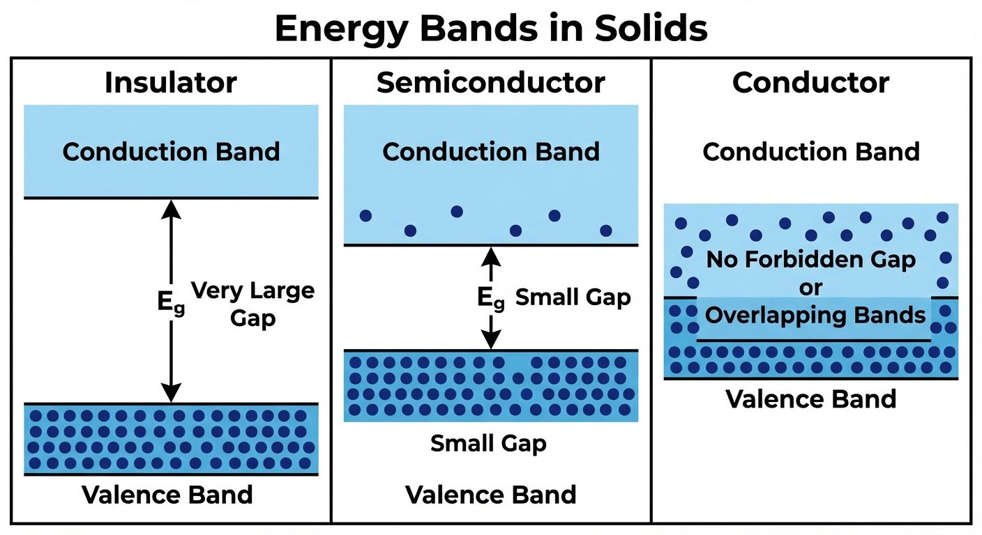
3. Theory of Solids: Band Theory
3.1 Formation of Allowed and Forbidden Energy Bands
- Isolated Atoms: In a single isolated atom, electrons occupy discrete, sharp energy levels.
- Crystal Formation: As atoms are brought together to form a solid lattice, the wave functions of outer electrons overlap. Due to the Pauli Exclusion Principle, discrete energy levels split into multiple closely spaced levels (N levels for N atoms).
- Bands: These closely spaced levels form continuous Energy Bands.
- Valence Band (VB): The band containing valence electrons (highest occupied band).
- Conduction Band (CB): The next higher band, which may be empty or partially filled. Electrons here are free to move.
- Forbidden Energy Gap (): The energy difference between the top of the VB and the bottom of the CB. No electrons can exist in this region.
3.2 Classification: Semiconductors and Insulators
Based on the band structure ():
-
Insulators:
- Very wide band gap ( eV, typically ~6 eV like Diamond).
- VB is full; CB is empty.
- Electrons cannot jump the gap at room temperature; hence, conductivity is negligible.
-
Semiconductors:
- Narrow band gap ( eV; Si = 1.1 eV, Ge = 0.7 eV).
- At 0K, they behave like insulators.
- At Room Temp, thermal energy excites some electrons from VB to CB, enabling conductivity.
-
Conductors (Metals):
- VB and CB overlap ().
- Electrons are always free to move.
3.3 Concept of Effective Mass
When an electron moves inside a periodic lattice, it interacts with the internal potential of the nuclei. It does not respond to external forces as a "free" particle of mass .
- Effective Mass (): A parameter that accounts for the internal forces within the crystal lattice. It relates external force to acceleration: .
- Mathematical Definition: Depends on the curvature of the (Energy-momentum) curve.
- Significance:
- Near the bottom of the CB, curvature is positive is positive (Electron).
- Near the top of the VB, curvature is negative is negative. This negative mass behavior is treated physically as a positive charge carrier called a Hole.
4. Semiconductor Physics
4.1 Fermi Level in Intrinsic and Extrinsic Semiconductors
A. Intrinsic (Pure) Semiconductors:
- Electron concentration () = Hole concentration ().
- The Fermi level lies exactly in the middle of the forbidden gap.
B. Extrinsic (Doped) Semiconductors:
Doping introduces impurity energy levels.
-
N-Type (Donor Doped):
- Pentavalent impurity (e.g., Phosphorus).
- Donates extra electrons.
- Donor energy level () forms just below the Conduction Band.
- Fermi Level: Shifts upward toward the Conduction Band ().
-
P-Type (Acceptor Doped):
- Trivalent impurity (e.g., Boron).
- Creates holes (vacancies).
- Acceptor energy level () forms just above the Valence Band.
- Fermi Level: Shifts downward toward the Valence Band ().
4.2 Direct vs. Indirect Band Gap Semiconductors
Based on the alignment of the Conduction Band minimum and Valence Band maximum in "k-space" (momentum space).
| Feature | Direct Band Gap | Indirect Band Gap |
|---|---|---|
| Structure | Max of VB and Min of CB occur at the same momentum value (). | Max of VB and Min of CB occur at different momentum values (). |
| Recombination | Electron falls directly to VB emitting a photon. | Electron needs a change in momentum (via lattice vibration/phonon) to recombine. |
| Emission | Emits light efficiently (Photons). | Energy released mostly as heat (Phonons). |
| Examples | GaAs (Gallium Arsenide), InP. | Si (Silicon), Ge (Germanium). |
| Uses | LEDs, Laser Diodes. | Rectifiers, Transistors. |
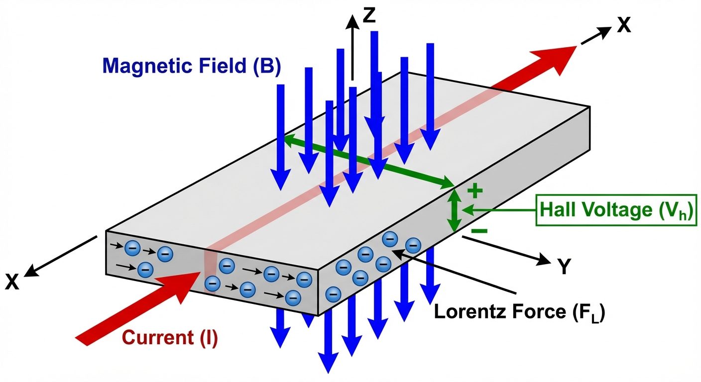
5. The Hall Effect
5.1 Definition
When a magnetic field () is applied perpendicular to a current-carrying conductor (), a voltage is developed across the specimen in a direction perpendicular to both the current and the magnetic field. This is called the Hall Voltage ().
5.2 Derivation
Consider a slab of semiconductor:
- Current flows in X-direction ().
- Magnetic field is in Z-direction ().
- Lorentz Force deflects carriers to the Y-direction.
- Magnetic Force (): Deflects carriers.
(magnitude) - Electric Force (): Accumulation of charge creates an internal electric field ().
- Equilibrium: Charges accumulate until electric force balances magnetic force.
- Current Density Relation:
- Hall Field:
- Hall Coefficient (): Defined as .
Final Hall Voltage Formula:
If is the width of the specimen ():
(Where is thickness).
5.3 Applications
- Determination of semiconductor type (N-type is negative; P-type is positive).
- Calculation of carrier concentration ().
- Calculation of carrier mobility ().
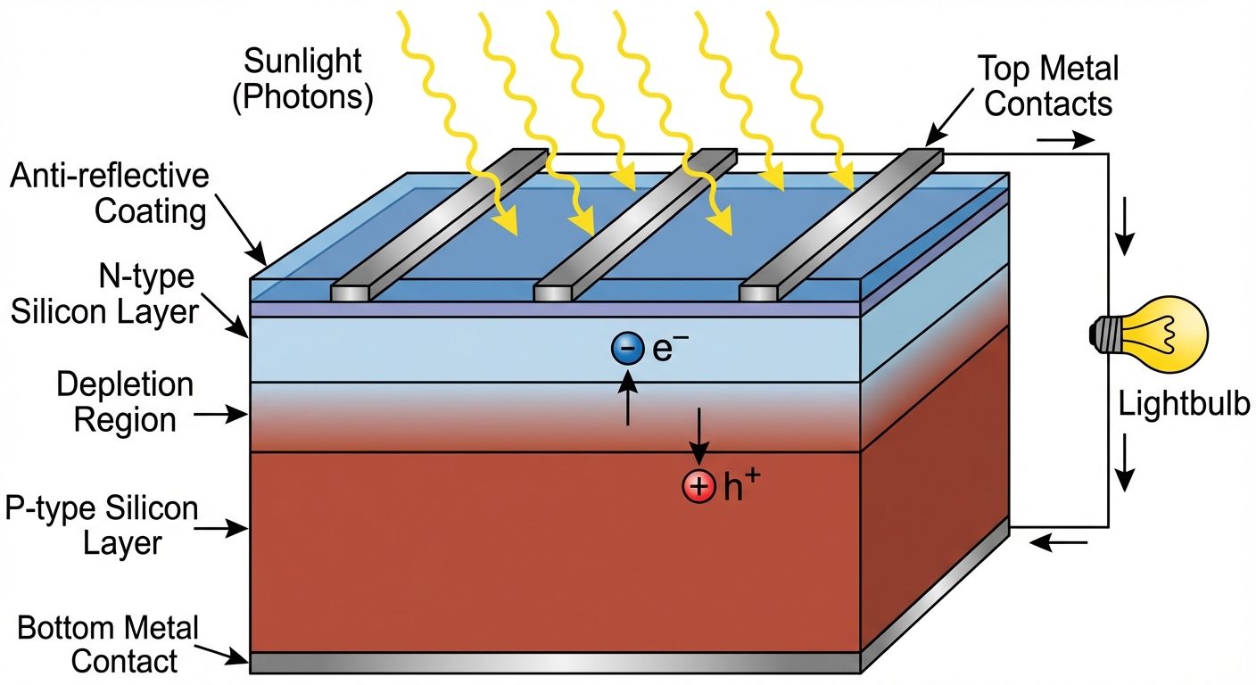
6. Solar Cell Basics
6.1 Principle
A solar cell (photovoltaic cell) is a P-N junction diode that converts light energy (photons) directly into electrical energy. It operates on the Photovoltaic Effect.
6.2 Working Mechanism
- P-N Junction: A junction is formed between P-type and N-type silicon. A depletion region forms with an internal electric field.
- Photon Absorption: When light with energy strikes the junction, photons are absorbed.
- Carrier Generation: The energy breaks bonds, generating Electron-Hole Pairs (EHPs).
- Separation: The internal electric field in the depletion region sweeps electrons toward the N-side and holes toward the P-side.
- Collection: This charge accumulation creates a potential difference (Open Circuit Voltage, ). If an external load is connected, current flows (Short Circuit Current, ).
6.3 I-V Characteristics
The solar cell operates in the fourth quadrant of the I-V characteristic curve (power is delivered, not consumed).
- (Open Circuit Voltage): Voltage when current is zero.
- (Short Circuit Current): Current when voltage is zero.
- Fill Factor (FF): A measure of the squareness of the I-V curve, indicating efficiency.