Unit 5 - Notes
Unit 5: Solid State Physics
1. Introduction to Free Electron Theory
The free electron theory attempts to explain the physical properties of metals, such as electrical and thermal conductivity.
Classical Free Electron Theory (Drude-Lorentz Model)
- Assumption: Valence electrons in a metal are "free" to move throughout the volume of the metal, behaving like the molecules of a perfect gas.
- Ion Cores: The positive ion cores (nuclei + inner shells) are fixed in lattice positions.
- Potentials: The mutual repulsion between electrons and attraction between electrons and ions are ignored. The potential is assumed to be constant everywhere inside the metal.
- Successes: Explains Ohm’s law and high electrical/thermal conductivity.
- Failures: Cannot explain the specific heat of metals, magnetic susceptibility, or the distinction between conductors, semiconductors, and insulators.
Quantum Free Electron Theory (Sommerfeld Model)
- Modifies the classical theory by applying quantum mechanics (Pauli Exclusion Principle and Fermi-Dirac statistics).
- Electrons are still free but confined to the metal (particle in a box).
- Energy levels are quantized.
2. Diffusion and Drift Current (Qualitative)
In semiconductors, current arises from two distinct mechanisms:
Drift Current
- Definition: The directed motion of charge carriers (electrons and holes) under the influence of an external electric field.
- Mechanism: When an electric field () is applied, carriers accelerate but collide with crystal lattice atoms, resulting in a constant average velocity called drift velocity ().
- Relationship: (Ohm's Law), where is current density and is conductivity.
Diffusion Current
- Definition: The flow of charge carriers from a region of higher concentration to a region of lower concentration.
- Mechanism: It is a random thermal motion process driven by a concentration gradient (), not by an electric field.
- Significance: Crucial in the operation of PN junction diodes and transistors where carrier injection creates non-uniform concentrations.
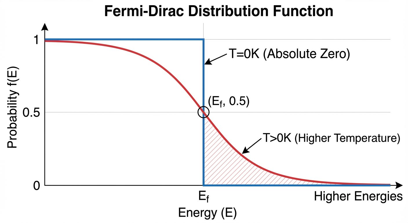
3. Fermi Energy and Fermi-Dirac Distribution
Fermi Energy ()
- Definition: At absolute zero temperature (), it is the highest energy level occupied by an electron.
- Physical Meaning: It represents the chemical potential of the electrons. At , it is the energy level where the probability of occupation is exactly 50% ($0.5$).
Fermi-Dirac Distribution Function ()
This function describes the probability that a specific energy state is occupied by an electron at absolute temperature .
Where:
- = Boltzmann constant
- = Absolute temperature
- = Fermi Energy
Behavior of :
- At :
- If , the exponential term is , so (All states full).
- If , the exponential term is , so (All states empty).
- This creates a sharp "step" function.
- At :
- Thermal energy excites some electrons across . The step function smooths out.
- At , .
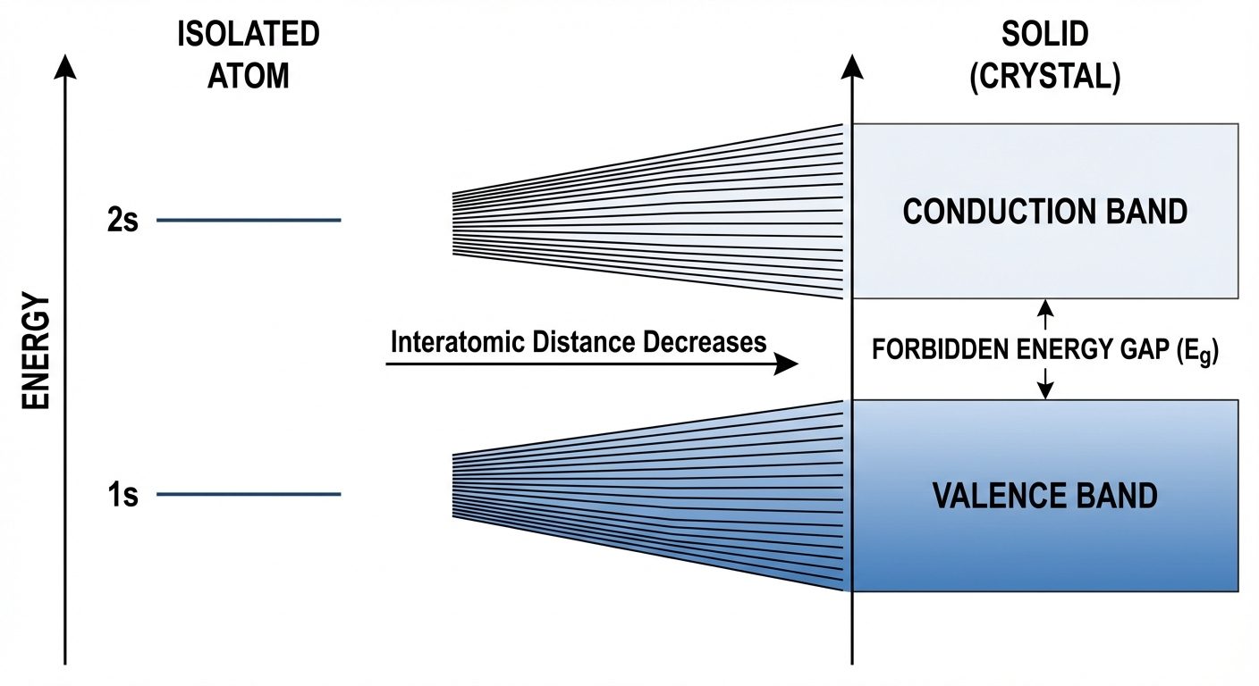
4. Theory of Solids: Formation of Energy Bands
Origin of Energy Bands
- Isolated Atoms: In a single isolated atom, electrons occupy discrete, sharp energy levels (1s, 2s, 2p, etc.).
- Approaching Atoms: As atoms are brought together to form a solid crystal, the wave functions of outer electrons overlap.
- Pauli Exclusion Principle: No two electrons can have the same quantum numbers. To satisfy this, the discrete energy levels split into closely spaced levels (where is the number of atoms).
- Band Formation: Since is huge (~), these discrete levels form a continuous continuum called an Energy Band.
Allowed and Forbidden Bands
- Valence Band (VB): The band containing valence electrons. It is the highest filled band at .
- Conduction Band (CB): The next higher energy band. Electrons here are free to move and conduct current.
- Forbidden Energy Gap (): The energy difference between the top of the valence band and the bottom of the conduction band. No allowed energy states exist in this region.
5. Classification of Solids
Solids are classified based on the width of the Forbidden Energy Gap ().
| Property | Insulators | Semiconductors | Conductors (Metals) |
|---|---|---|---|
| Band Gap () | Large () | Small () | Zero (Overlapping) |
| Valence Band | Completely Full | Almost Full | Partially Full |
| Conduction Band | Completely Empty | Almost Empty | Overlaps with VB |
| Conductivity | Negligible | Moderate (Increases with T) | High (Decreases with T) |
| Examples | Diamond, Glass, Wood | Silicon (), Germanium () | Copper, Aluminum, Silver |
6. Concept of Effective Mass
Inside a crystal, an electron moves under the influence of the internal periodic potential of the lattice, not just external fields. To treat the electron as a "free" particle in classical equations (like ), we replace its rest mass () with Effective Mass ().
- Definition: The mass that a particle seems to possess when responding to forces within the crystal lattice. It relates to the curvature of the energy band ( diagram).
- Physical Significance:
- High Curvature (Steep Parabola): Small effective mass (electron moves easily).
- Low Curvature (Flat Band): Large effective mass (electron is "heavy" and sluggish).
Electrons and Holes
- Electrons (CB): Found near the bottom of the conduction band (positive curvature, positive mass).
- Holes (VB): Found near the top of the valence band. The effective mass is negative mathematically, but they behave as positive charge carriers with positive effective mass in an electric field.
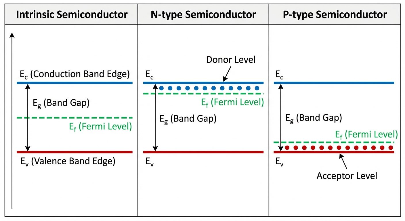
7. Fermi Level in Intrinsic and Extrinsic Semiconductors
Intrinsic Semiconductors (Pure)
- Electron density () = Hole density ().
- Fermi Level (): Lies exactly in the middle of the forbidden gap.
Extrinsic Semiconductors (Doped)
- N-Type (Pentavalent doping):
- Donor impurities add electrons.
- Fermi Level: Shifts upward, towards the Conduction Band ().
- At , is exactly between the donor level () and .
- P-Type (Trivalent doping):
- Acceptor impurities create holes.
- Fermi Level: Shifts downward, towards the Valence Band ().
- At , is exactly between the acceptor level () and .
8. Direct and Indirect Band Gap Semiconductors
The classification depends on the alignment of the minimum of the Conduction Band () and the maximum of the Valence Band () in momentum space (-space).
Direct Band Gap
- Structure: The minimum of the CB and maximum of the VB occur at the same value of wave vector (usually ).
- Transition: An electron can recombine with a hole directly by emitting a photon. Conservation of momentum is satisfied naturally.
- Application: LEDs, Laser Diodes.
- Example: Gallium Arsenide (GaAs).
Indirect Band Gap
- Structure: The minimum of the CB and maximum of the VB occur at different values of .
- Transition: Direct recombination is not possible because momentum () would not be conserved. Recombination requires a phonon (lattice vibration) to mediate the momentum change, releasing energy mostly as heat, not light.
- Application: Rectifiers, Transistors (poor for light emission).
- Example: Silicon (Si), Germanium (Ge).
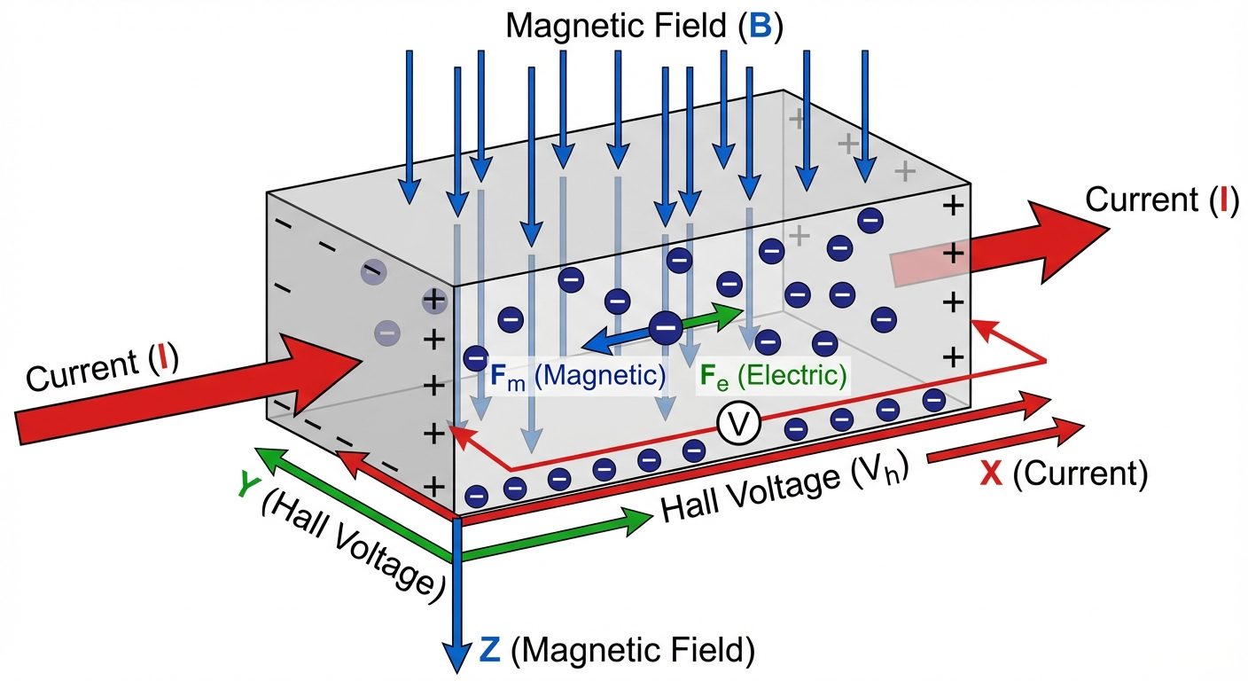
9. The Hall Effect
Definition: When a current-carrying conductor or semiconductor is placed in a transverse magnetic field, an electric field (Hall field) is induced perpendicular to both the current and the magnetic field.
Derivation
Consider a semiconductor slab of width and thickness .
- Current (): Flows along the X-axis.
- Magnetic Field (): Applied along the Z-axis.
- Lorentz Force: Charge carriers moving with drift velocity experience a magnetic force downwards (Y-axis):
- Accumulation: Electrons accumulate at the bottom face, creating a negative charge. The top face becomes positive.
- Hall Electric Field (): This charge separation creates an electric field upwards, exerting an electric force on carriers:
- Equilibrium: Charges accumulate until electric force balances magnetic force:
- Hall Voltage (): Since (where is the width across which voltage is measured):
- Current Density (): . Therefore, .
(Note: Sometimes area is defined by thickness . If width is and thickness is , ). Let's assume standard area .
- Hall Coefficient ():
Substituting into the equation:
Applications
- Determination of semiconductor type (N-type or P-type) based on the sign of .
- Calculation of carrier concentration ().
- Determination of mobility ().
- Magnetic field meters (Hall sensors).
10. Solar Cell Basics
A solar cell is a PN junction diode that converts optical energy (sunlight) directly into electrical energy via the Photovoltaic Effect.
Principle
It operates on the principle of electron-hole pair generation by photon absorption. No external bias is applied.
Working Mechanism
- Absorption: Light photons with energy strike the solar cell.
- Generation: Photons are absorbed in the depletion region (or close to it), generating electron-hole pairs.
- Separation: The built-in electric field of the depletion region separates the carriers before they recombine.
- Electrons are swept to the N-side.
- Holes are swept to the P-side.
- Collection: This accumulation of charges creates a voltage (Open Circuit Voltage, ). If a load is connected, current () flows.
I-V Characteristics
- The solar cell operates in the fourth quadrant of the I-V characteristic curve (generates power).
- (Open Circuit Voltage): Voltage when current is zero.
- (Short Circuit Current): Current when voltage is zero.
- Fill Factor (FF): A measure of the squareness of the I-V curve, determining efficiency.