Practical 6
Practical 6: Flip-Flop Warriors: NAND Edition
1. Aim/Objective
To design, construct, and validate the logic and operation of a JK Flip-Flop using discrete NAND gates (Universal Logic Gates).
2. Apparatus/Components Required
| Component | Specification/Type | Quantity |
|---|---|---|
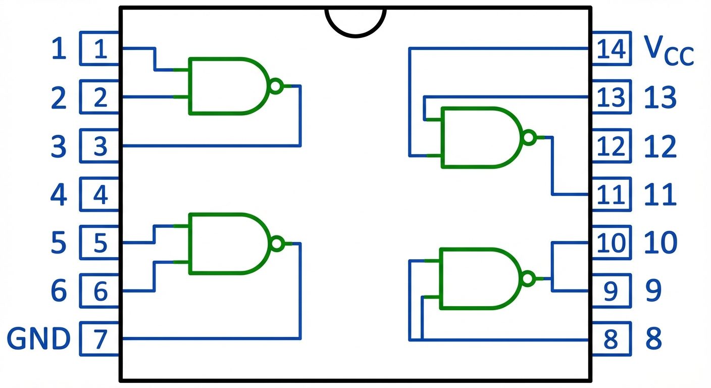
| IC 7400 | Quad 2-Input NAND Gate | 1 |
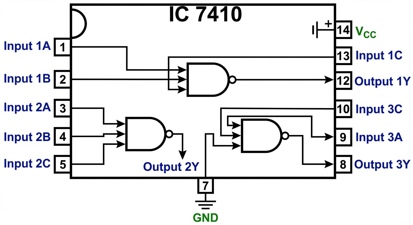
| IC 7410 | Triple 3-Input NAND Gate | 1 |
| Breadboard | Standard | 1 |
| DC Power Supply | +5V Regulated | 1 |
| LEDs | Red (Output Q), Green (Output Q') | 2 |
| Resistors | 220 or 330 | 2 |
| Connecting Wires | Single strand / jumper wires | As req. |
| Logic Inputs | Toggle switches or DIP switches | 3 (J, K, Clk) |
3. Theory
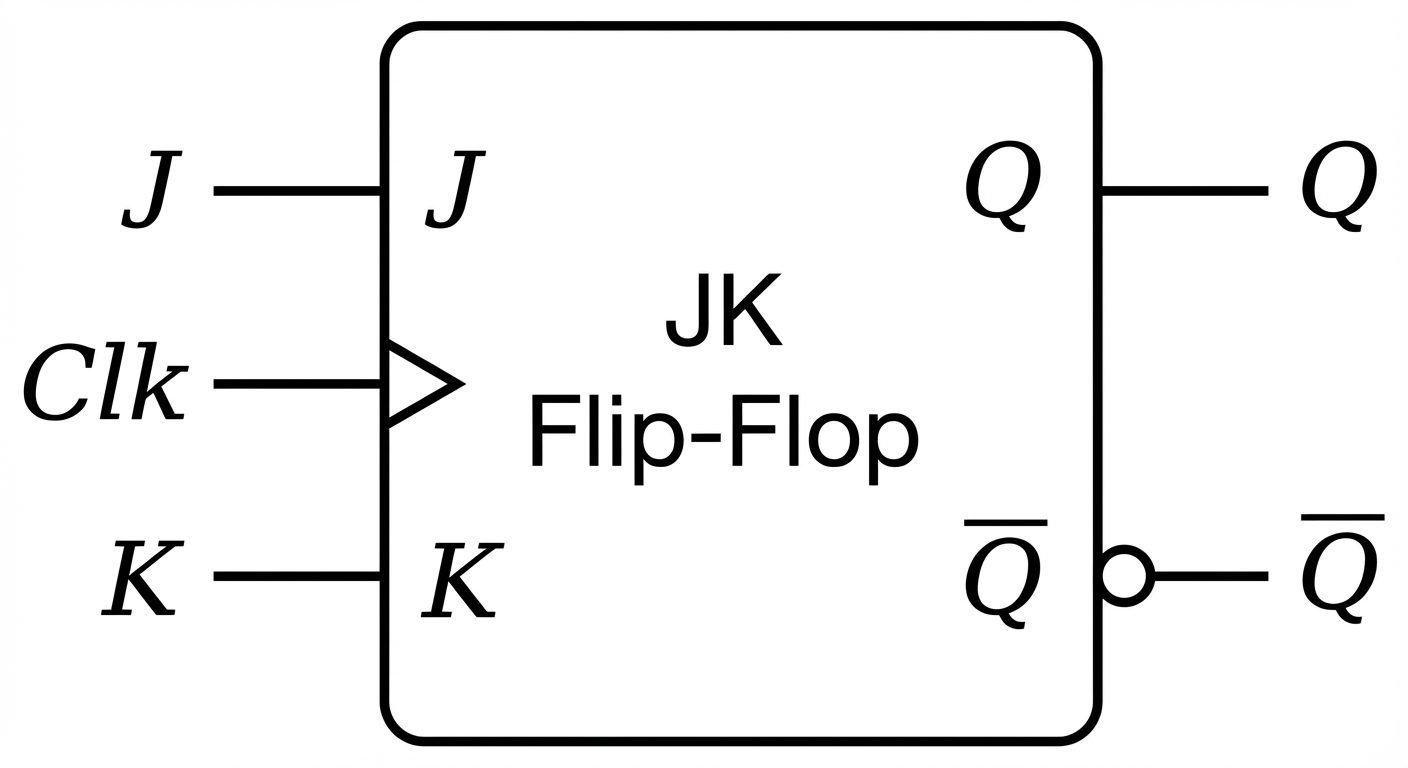
3.1 The JK Flip-Flop
The JK Flip-Flop is considered the "universal" flip-flop because it eliminates the invalid state found in SR flip-flops. It has two data inputs (J and K) and a Clock input (Clk).
- J (Jack): Acts like the Set input.
- K (King): Acts like the Reset input.
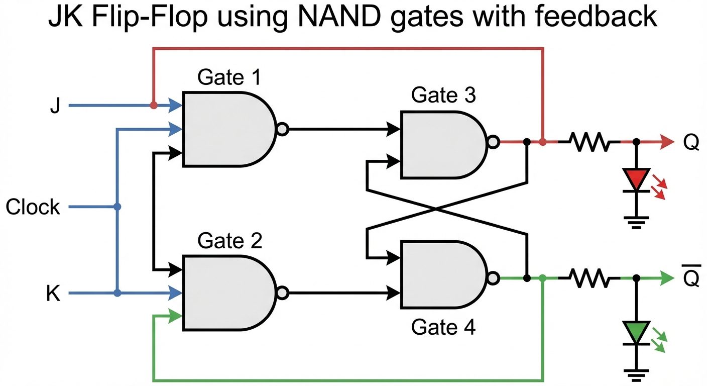
- Feedback: The outputs and are fed back to the inputs to enable the toggling action.
3.2 Logic with NAND Gates
To construct a JK Flip-Flop using NAND gates, we require:
- A Memory Cell (Latch): Formed by two cross-coupled 2-input NAND gates (using IC 7400).
- Steering/Input Logic: Formed by two 3-input NAND gates (using IC 7410).
The 3-input gates accept the Input (J or K), the Clock, and the Feedback from the opposing output.
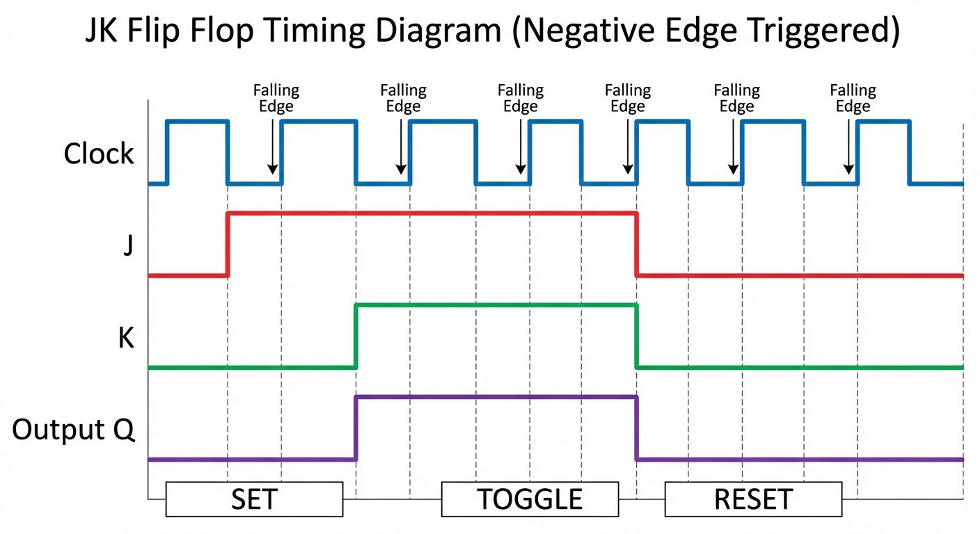
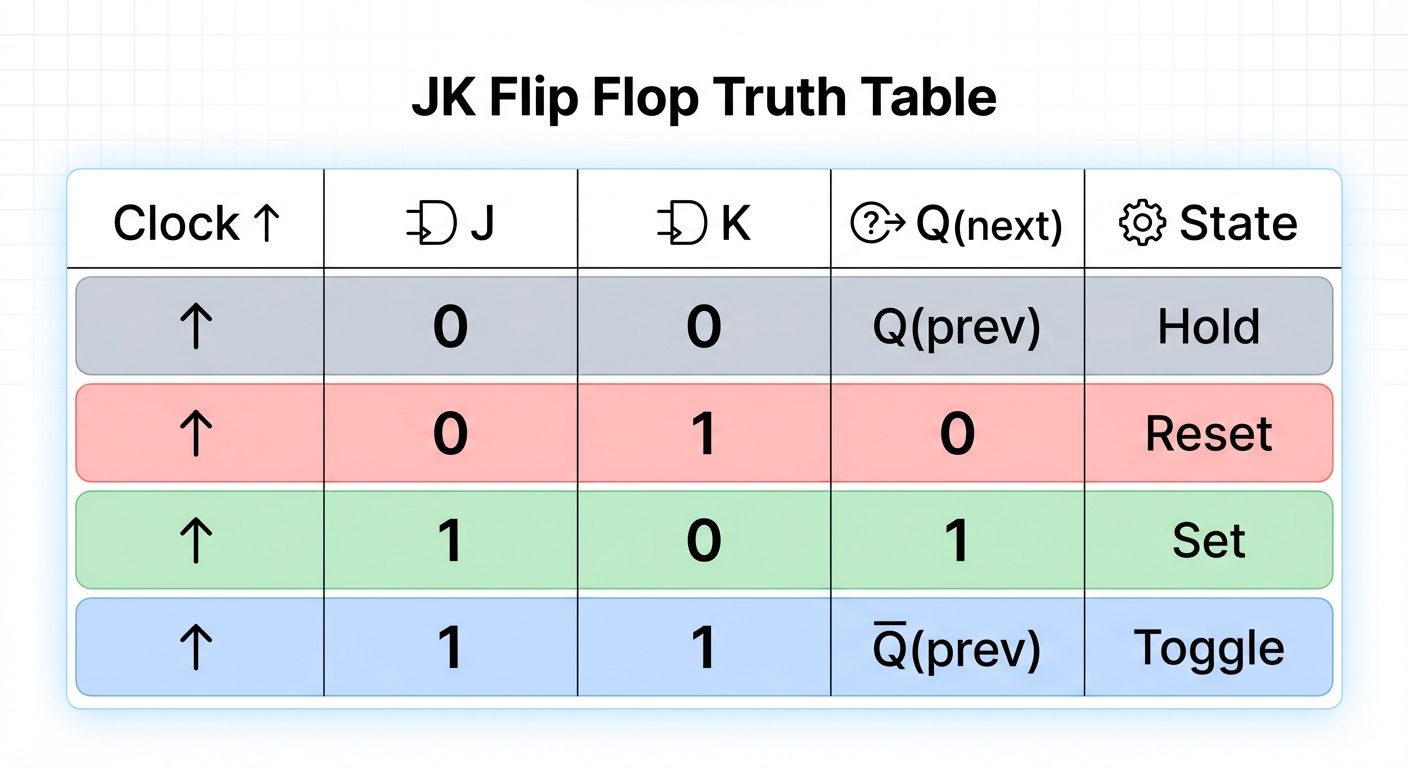
3.3 The Operation States
- Hold State (): No change in output ().
- Reset State (): The flip-flop resets ().
- Set State (): The flip-flop sets ().
- Toggle State (): The output switches to its complement ().
Note: In a basic level-triggered circuit constructed on a breadboard, the Toggle state may result in a "Race-Around Condition" where the output oscillates while the clock is high. This confirms the logic, though practical applications usually use Master-Slave configurations.
4. Pin Diagrams
To build this circuit, familiarity with the pin configurations of the 7400 and 7410 series ICs is essential.
5. Circuit Diagram / Setup
The circuit utilizes two gates from the IC 7410 and two gates from the IC 7400.
Connections:
- Gate 1 (IC 7410): Inputs are J, Clk, and Feedback from . Output goes to the Set input of the latch.
- Gate 2 (IC 7410): Inputs are K, Clk, and Feedback from Q. Output goes to the Reset input of the latch.
- Gate 3 & 4 (IC 7400): Cross-coupled to form the SR Latch.
6. Procedure
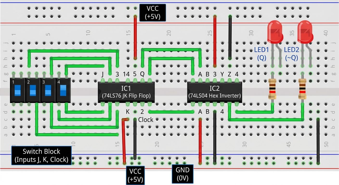
- Placement: Insert IC 7400 and IC 7410 into the breadboard groove firmly.
- Power: Connect Pin 14 of both ICs to +5V (Vcc) and Pin 7 of both ICs to Ground (GND).
- Latch Construction (Using IC 7400):
- Connect Output Pin 3 to Input Pin 5.
- Connect Output Pin 6 to Input Pin 2.
- Note: Using Gate 1 (Pins 1,2,3) and Gate 2 (Pins 4,5,6) of 7400.
- Connect Pin 1 to the output of the J-steering gate.
- Connect Pin 4 to the output of the K-steering gate.
- Steering Logic (Using IC 7410):
- J-Gate: Use pins 1, 2, 13 (Inputs) and 12 (Output). Connect Pin 12 to Pin 1 of IC 7400.
- K-Gate: Use pins 3, 4, 5 (Inputs) and 6 (Output). Connect Pin 6 to Pin 4 of IC 7400.
- Feedback Connections:
- Connect Output Q (Pin 3 of 7400) back to an input of the K-Gate (Pin 5 of 7410).
- Connect Output (Pin 6 of 7400) back to an input of the J-Gate (Pin 13 of 7410).
- Inputs: Connect switches to J (Pin 1 of 7410), K (Pin 3 of 7410), and Clock (Pin 2 and Pin 4 of 7410 tied together).
- Outputs: Connect LED (via 330 resistor) to Pin 3 of 7400 (Q) and Pin 6 of 7400 ().
- Validation: Apply the logic combinations as per the observation table and record the LED status.
7. Observations / Truth Table
Notation:
- : Current State
- : Next State
- Logic 0 = LED OFF (0V)
- Logic 1 = LED ON (+5V)
- Clk: Logic High Pulse
| Clock (Clk) | Input J | Input K | Present State () | Next State () | Action/Mode |
|---|---|---|---|---|---|
| 0 | X | X | 0 | 0 | No Change |
| 0 | X | X | 1 | 1 | No Change |
| (1) | 0 | 0 | 0 | 0 | Hold |
| (1) | 0 | 0 | 1 | 1 | Hold |
| (1) | 0 | 1 | 0 | 0 | Reset |
| (1) | 0 | 1 | 1 | 0 | Reset |
| (1) | 1 | 0 | 0 | 1 | Set |
| (1) | 1 | 0 | 1 | 1 | Set |
| (1) | 1 | 1 | 0 | 1 | Toggle |
| (1) | 1 | 1 | 1 | 0 | Toggle |
8. Result
The JK Flip-Flop was successfully designed using NAND gates (IC 7400 and IC 7410). The logic states (Hold, Set, Reset, and Toggle) were verified against the theoretical truth table.
Conclusion on Toggle State: When and , the output toggles. However, due to the continuous clock pulse in this discrete setup, a "Race-Around" condition may be observed (LEDs appearing dim or flickering) indicating the output is oscillating while the clock is high.
9. Viva Questions
Q1. Why is the JK Flip-Flop called a "Universal" Flip-Flop?
Ans: It is versatile and solves the indeterminate/invalid state problem of the SR flip-flop. It can also be configured to act as a D flip-flop or T flip-flop.
Q2. What is the "Race-Around Condition"?
Ans: In a level-triggered JK flip-flop, if and the clock pulse width () is greater than the propagation delay of the gates, the output will toggle multiple times within a single clock pulse. This is an unwanted oscillation.
Q3. How do we eliminate the Race-Around Condition?
Ans: By using a Master-Slave JK Flip-Flop configuration or by using edge-triggered flip-flops where the pulse width is effectively negligible.
Q4. What is the function of the Clear (CLR) and Preset (PRE) pins found on standard JK Flip-Flop ICs (like 7476)?
Ans: These are asynchronous inputs. PRE sets immediately irrespective of the Clock. CLR resets immediately irrespective of the Clock.
Q5. Can we realize this circuit using only IC 7400 (2-input NANDs)?
Ans: Yes, but it is more complex. You would need to construct the 3-input NAND function using two 2-input NANDs (cascading them), requiring more gates and wiring.