Practical 5
Practical 5: Adder Chronicles
1. Aim/Objective
To design, construct, and verify the combinational logic circuits for:
- A Half Adder using XOR and AND gates.
- A Full Adder using two Half Adders and an OR gate.
To verify the truth tables of both circuits by observing the logic states of the outputs.
2. Apparatus/Components Required
- Digital IC Trainer Kit or Breadboard with +5V DC Power Supply.
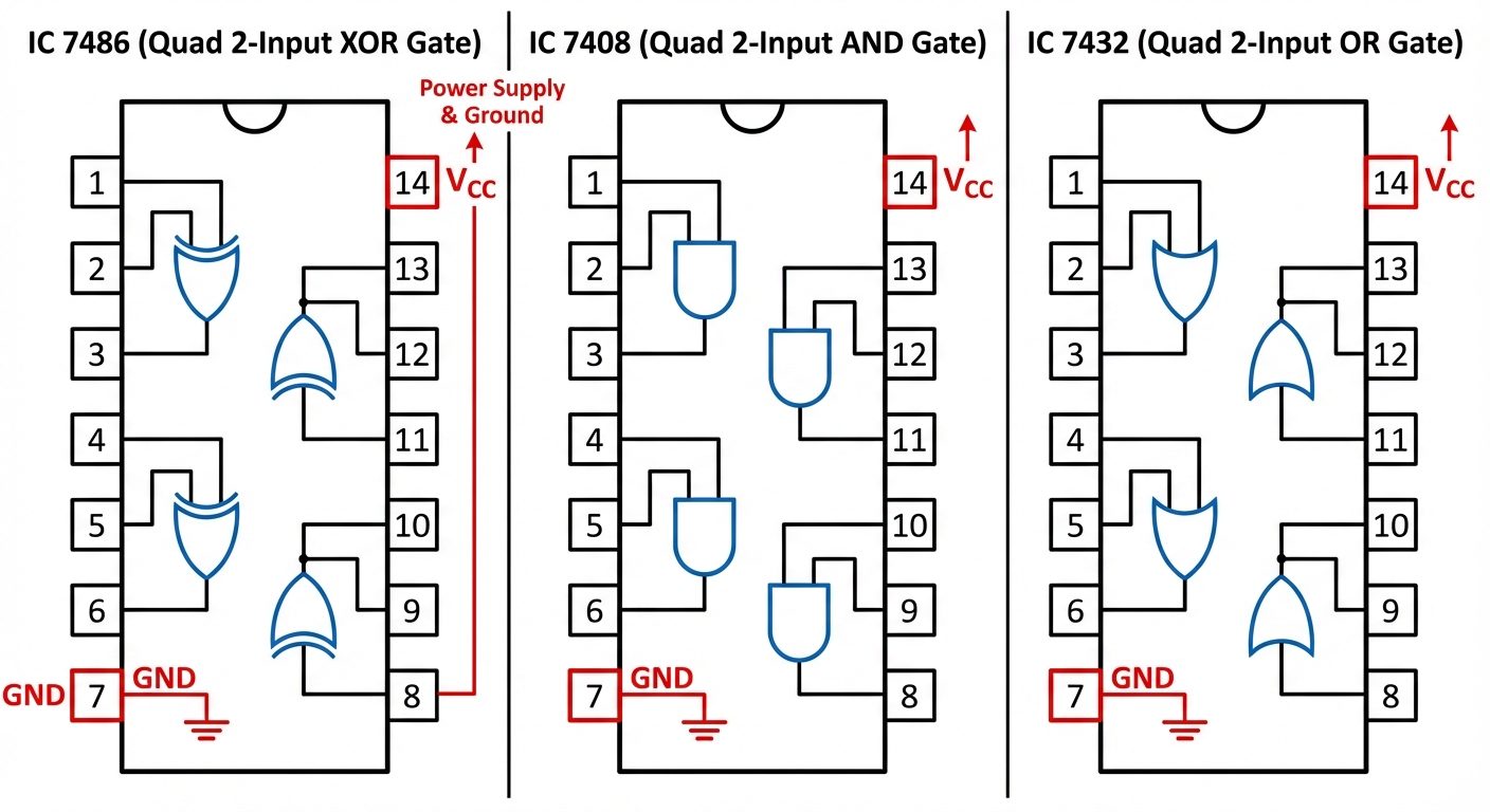
- Integrated Circuits (ICs):
- IC 7486 (Quad 2-input XOR gate)
- IC 7408 (Quad 2-input AND gate)
- IC 7432 (Quad 2-input OR gate)
- LEDs (Light Emitting Diodes) – 2 qty (for Output indication).
- Resistors – 330 or 220 (for LED current limiting).
- Connecting Wires (Single strand hook-up wire).
- Logic Probes or Multimeter (optional, for debugging).
3. Theory
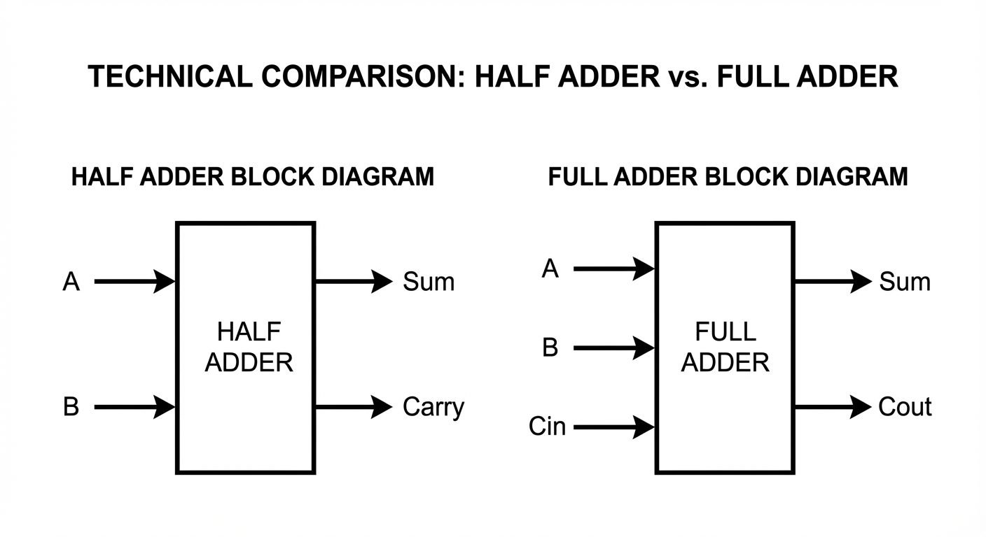
Half Adder
A Half Adder is a combinational circuit that performs the addition of two single-bit binary numbers. It has two inputs, A (Augend) and B (Addend), and two outputs, S (Sum) and C (Carry).
Boolean Expressions:
- Sum (S) = (A XOR B)
- Carry (C) = (A AND B)
The limitation of the half adder is that it cannot accept a carry bit from a previous stage, making it insufficient for multi-bit addition on its own.
Full Adder
A Full Adder is a combinational circuit that performs the addition of three single-bit binary numbers. It has three inputs: A, B, and (Carry input from the previous stage), and two outputs: S (Sum) and (Carry output).
Boolean Expressions:
- Sum (S) =
- Carry () =
A Full Adder can be constructed using two Half Adders and one OR gate.
4. Pin Configurations
Before making connections, observe the pinout diagrams for the logic gates used. All ICs used here are 14-pin DIP packages.
- Pin 7: Ground (GND)
- Pin 14: Supply (+5V VCC)
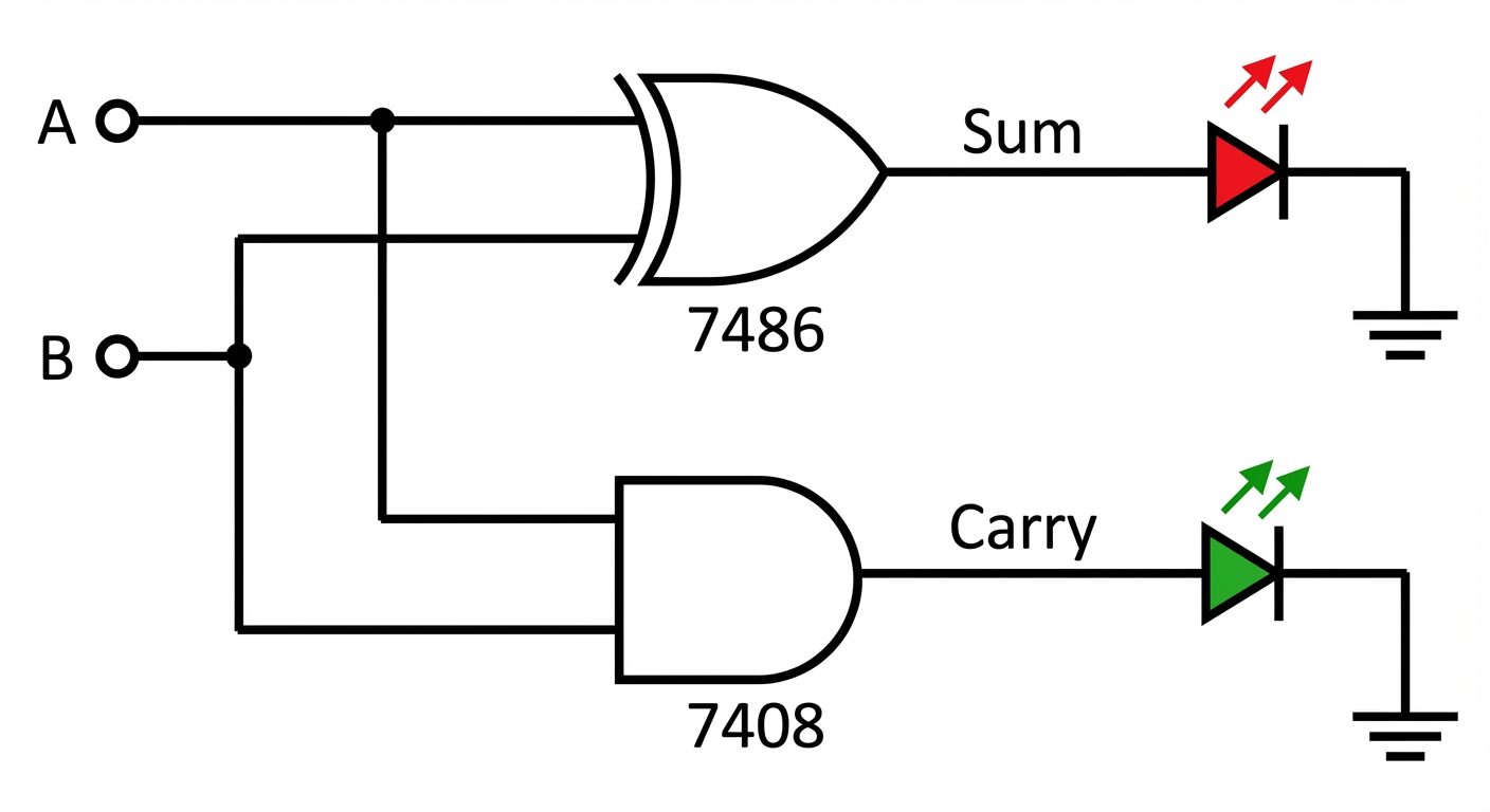
5. Part A: Half Adder
Circuit Diagram
Procedure
- Place IC 7486 (XOR) and IC 7408 (AND) on the breadboard.
- Connect Pin 7 of both ICs to Ground and Pin 14 of both ICs to +5V VCC.
- Connect Input A to Pin 1 of IC 7486 and Pin 1 of IC 7408.
- Connect Input B to Pin 2 of IC 7486 and Pin 2 of IC 7408.
- Connect the Sum output (Pin 3 of IC 7486) to an LED via a series resistor.
- Connect the Carry output (Pin 3 of IC 7408) to a second LED via a series resistor.
- Apply various combinations of inputs (Logic 0 = GND, Logic 1 = +5V) according to the truth table.
- Observe the status of LEDs (ON = Logic 1, OFF = Logic 0).
6. Part B: Full Adder
Circuit Diagram
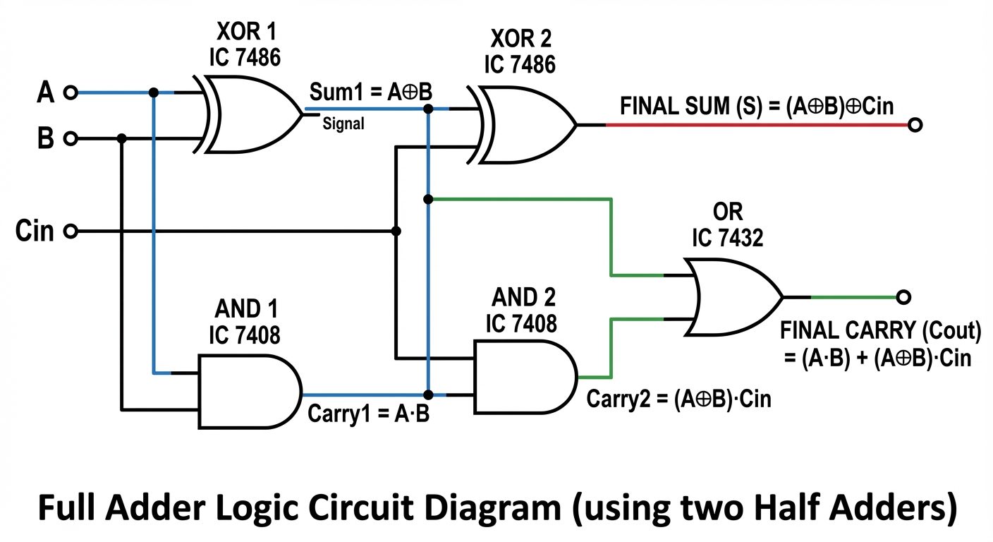
Wiring Layout (Visual Aid)
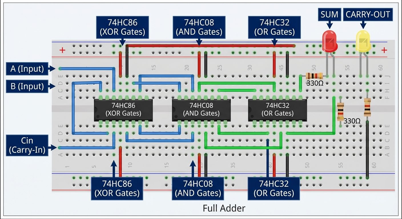
Procedure
- Place IC 7486, IC 7408, and IC 7432 on the breadboard.
- Power: Connect Pin 7 of all ICs to GND and Pin 14 of all ICs to +5V.
- First Half Adder Stage:
- Connect Inputs A and B to pins 1 and 2 of the first XOR gate (7486) and pins 1 and 2 of the first AND gate (7408).
- Second Half Adder Stage:
- Take the output of the first XOR (Pin 3) and connect it to one input of the second XOR (e.g., Pin 4 of 7486).
- Connect the third input to the other input of the second XOR (Pin 5 of 7486).
- The output of this second XOR (Pin 6 of 7486) is the final SUM. Connect to LED.
- Carry Logic Generation:
- Connect the output of the first XOR (Pin 3 of 7486) to an input of the second AND gate (e.g., Pin 4 of 7408).
- Connect to the other input of that AND gate (Pin 5 of 7408).
- Take the output of the first AND gate (Pin 3 of 7408) and the output of the second AND gate (Pin 6 of 7408).
- Connect these two outputs to the inputs of the OR gate (Pins 1 and 2 of IC 7432).
- The output of the OR gate (Pin 3 of 7432) is the final CARRY (). Connect to LED.
- Verify all 8 input combinations as per the truth table.
7. Observations and Truth Tables
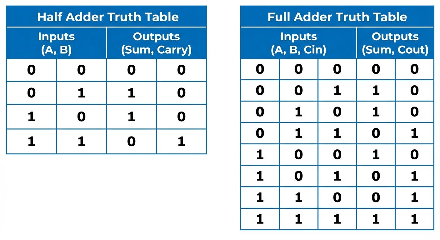
Table 1: Half Adder
| Input A | Input B | Sum () | Carry () |
|---|---|---|---|
| 0 | 0 | 0 | 0 |
| 0 | 1 | 1 | 0 |
| 1 | 0 | 1 | 0 |
| 1 | 1 | 0 | 1 |
Table 2: Full Adder
| Input A | Input B | Input | Sum (S) | Carry () |
|---|---|---|---|---|
| 0 | 0 | 0 | 0 | 0 |
| 0 | 0 | 1 | 1 | 0 |
| 0 | 1 | 0 | 1 | 0 |
| 0 | 1 | 1 | 0 | 1 |
| 1 | 0 | 0 | 1 | 0 |
| 1 | 0 | 1 | 0 | 1 |
| 1 | 1 | 0 | 0 | 1 |
| 1 | 1 | 1 | 1 | 1 |
(Note: Verify these logic levels. If LED is ON, record '1'. If LED is OFF, record '0'.)
8. Result
The Half Adder and Full Adder circuits were successfully designed and constructed on the breadboard. The output logic states for Sum and Carry were observed for all input combinations, and the truth tables were verified to match theoretical predictions.
9. Viva Questions
- What is the main limitation of a Half Adder?
- Answer: A Half Adder cannot accept a Carry input () from a previous lower-significant bit addition, making it unsuitable for cascading in multi-bit addition.
- How many NAND gates are required to implement a Half Adder?
- Answer: It requires 5 NAND gates to implement a Half Adder.
- Why do we use the XOR gate for the Sum output?
- Answer: The Sum output in binary addition follows the logic of inequality (outputs 1 only when inputs are different, or odd number of 1s in Full Adder), which corresponds exactly to the XOR operation.
- Write the expression for the Carry of a Full Adder in terms of Minterms.
- Answer: or .
- Can we implement a Full Adder using two Half Adders?
- Answer: Yes, a Full Adder consists of two Half Adders and one OR gate.
- What is a Ripple Carry Adder?
- Answer: It is a circuit where multiple Full Adders are cascaded in series, with the Carry Output of one stage connected to the Carry Input of the next stage.
- What is the propagation delay in an adder circuit?
- Answer: It is the time taken for the input signal change to produce a stable change at the output. In ripple adders, this delay accumulates through each stage.