Practical 4
Practical 4: Universal Gate Adventure
1. Aim/Objective
To design, implement, and verify the functionality of basic logic gates (NOT, AND, OR) using only Universal Gates (NAND and NOR).
2. Apparatus/Components Required
| Component/Equipment | Specification/Details | Quantity |
|---|---|---|
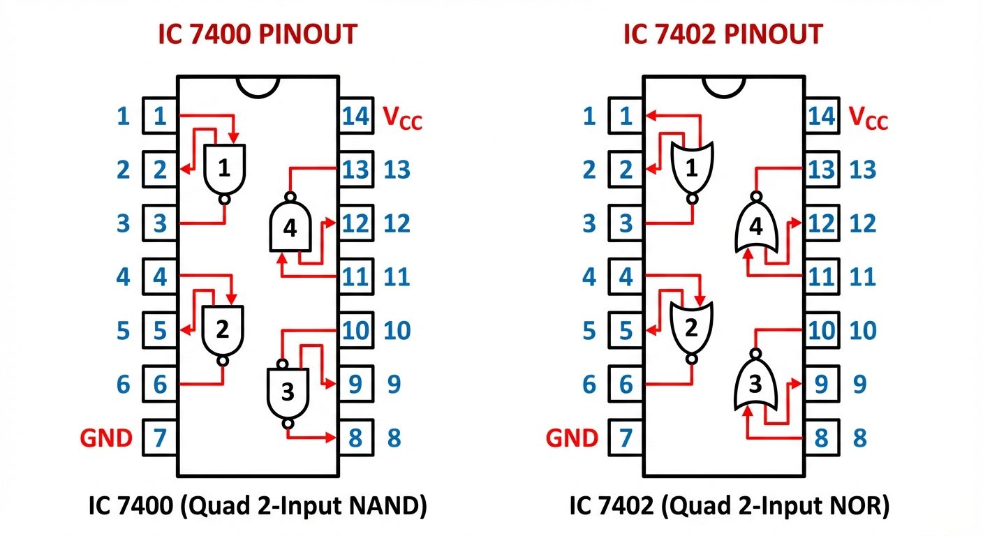
| IC 7400 | Quad 2-input NAND Gate (TTL) | 1 |
| IC 7402 | Quad 2-input NOR Gate (TTL) | 1 |
| DC Power Supply | +5V Regulated | 1 |
| Digital Trainer Kit | Optional (or use Breadboard) | 1 |
| Breadboard | Solderless | 1 |
| LEDs | 5mm (Red/Green) for Output | 2-3 |
| Resistors | 330Ω or 470Ω (Current Limiting) | 2-3 |
| Connecting Wires | Single strand hook-up wires | As req. |
3. Theory
A Universal Gate is a logic gate that can be used to construct any other logic gate (AND, OR, NOT, XOR, XNOR). The two universal gates are NAND and NOR.
3.1 NAND Gate (IC 7400)
The NAND operation represents an AND operation followed by a NOT operation.
- Symbol: AND gate with a bubble at the output.
- Expression:
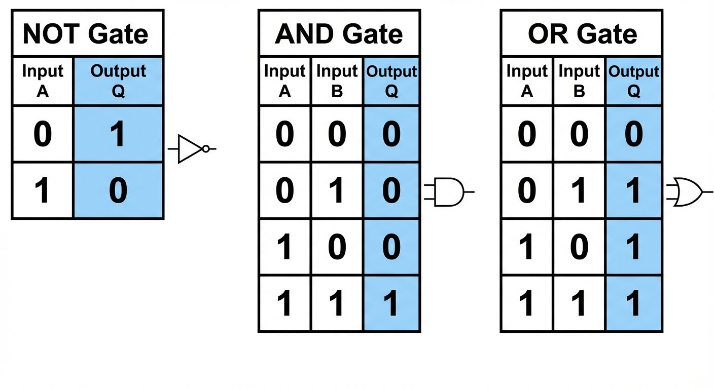
- Logic: The output is LOW (0) only when all inputs are HIGH (1).
3.2 NOR Gate (IC 7402)
The NOR operation represents an OR operation followed by a NOT operation.
- Symbol: OR gate with a bubble at the output.
- Expression:
- Logic: The output is HIGH (1) only when all inputs are LOW (0).
3.3 Designing Basic Gates using Universal Gates
By using De Morgan's Laws and boolean algebra, we can configure these gates to perform basic functions:
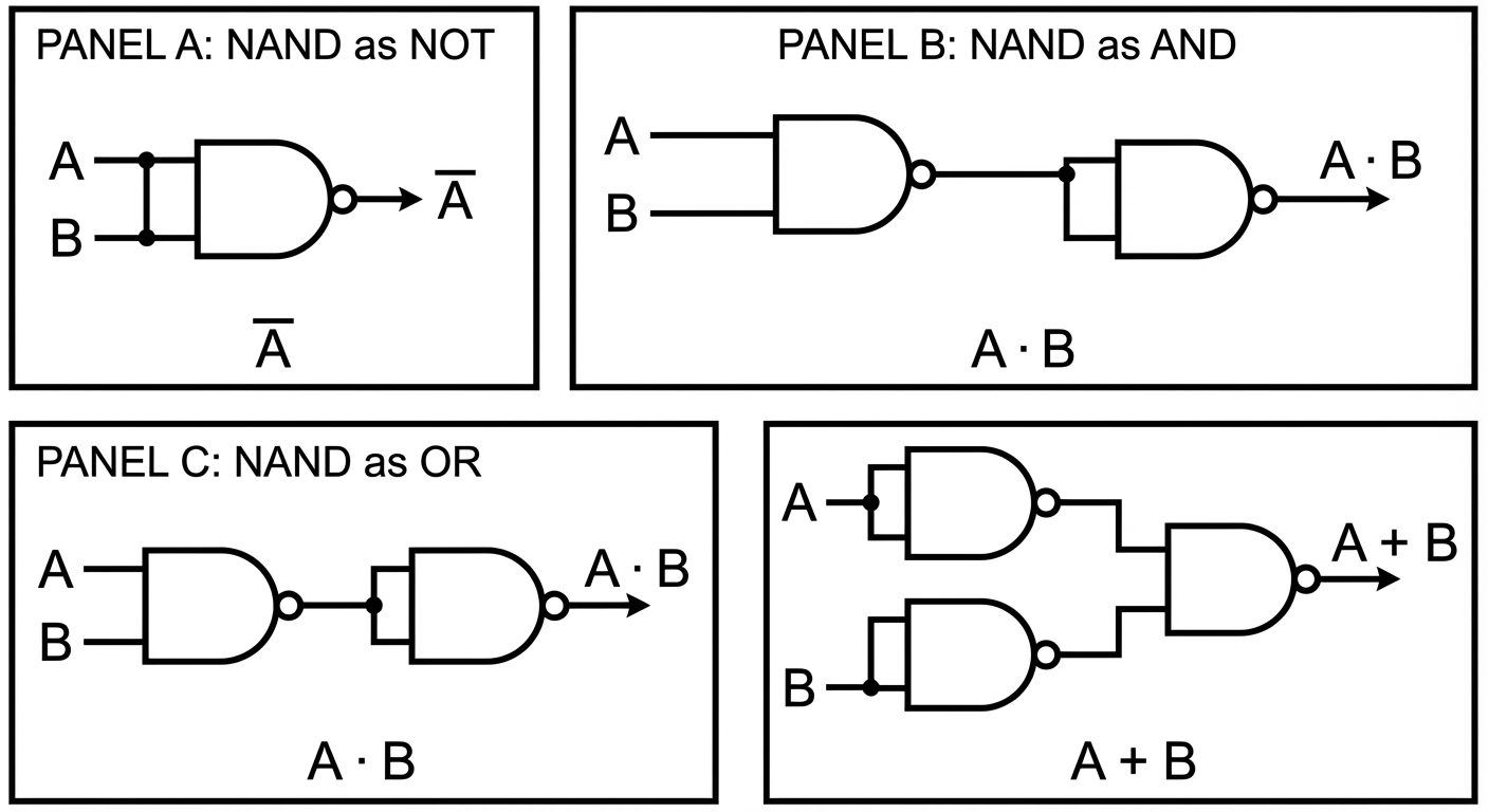
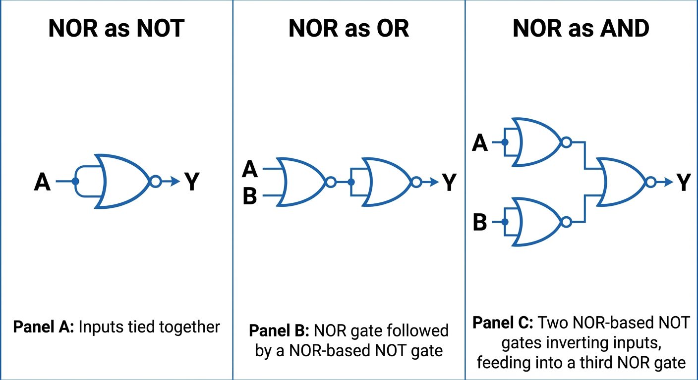
- NOT Gate: Connect both inputs of a NAND/NOR gate together ().
- AND Gate: Connect a NAND gate followed by a NOT gate (made of NAND).
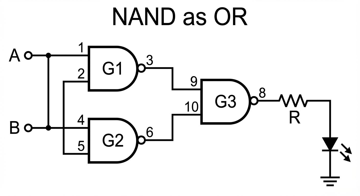
- OR Gate: Invert inputs A and B individually using NANDs, then feed them into a third NAND gate.
4. Pin Diagrams and Circuit Setup
Before making connections, it is crucial to understand the pin configuration of the ICs. Note that while IC 7400 follows a standard Input-Input-Output pattern, IC 7402 is different (Output-Input-Input).
4.1 Implementation Logic
Below are the connection schematics for the experiment.
Part A: Using NAND (IC 7400)
- NOT Logic: Input to Pins 1 & 2 (shorted); Output at Pin 3.
- AND Logic: Gate 1 (Pins 1,2 Input) Output Pin 3 Input to Gate 2 (Pins 4,5 shorted) Final Output Pin 6.
- OR Logic: Gate 1 (Invert A), Gate 2 (Invert B) Gate 3 (NAND the inverted inputs).
Part B: Using NOR (IC 7402)
The logic is the dual of NAND.
- NOT Logic: Input to Pins 2 & 3 (shorted); Output at Pin 1.
- OR Logic: NOR followed by NOT (made of NOR).
- AND Logic: Invert inputs A and B individually using NORs, then feed to a third NOR.
5. Procedure
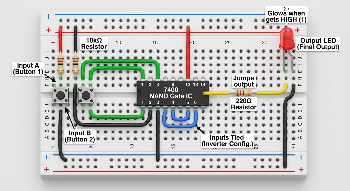
- Preparation: Place the IC 7400 on the breadboard. Ensure the notch faces the left.
- Power: Connect Pin 14 to +5V Vcc and Pin 7 to Ground (GND). Do not reverse polarity.
- Part A: NAND Implementation
- NOT Gate: Short pins 1 and 2 using a jumper wire. Connect this junction to an input switch (Input A). Connect Pin 3 (Output) to an LED via a 330Ω resistor. Toggle A and record the LED status.
- AND Gate: Connect inputs A and B to pins 1 and 2. Connect pin 3 to pins 4 and 5 (shorted together). Connect pin 6 to the LED. Verify the truth table.
- OR Gate: Construct the circuit as shown in the specific schematic (Theory section 3.3). Use three gates inside the IC.
- Part B: NOR Implementation
- Remove IC 7400 and insert IC 7402. Connect Vcc (14) and GND (7).
- Note: Remember that for 7402, Pin 1 is Output, and Pins 2 & 3 are Inputs.
- Repeat the logic design steps using the NOR logic defined in the Theory section.
- Validation: For each setup, apply logic combinations (00, 01, 10, 11) and observe the LED.
- LED ON = Logic High (1)
- LED OFF = Logic Low (0)
6. Observations and Truth Tables
6.1 Realization using NAND Gates (IC 7400)
| Table 1: NAND as NOT | Input (A) | Expected Output () | Observed Output (LED) |
|---|---|---|---|
| 0 | 1 | ON | |
| 1 | 0 | OFF |
| Table 2: NAND as AND | Input A | Input B | Expected Output () | Observed Output (LED) |
|---|---|---|---|---|
| 0 | 0 | 0 | OFF | |
| 0 | 1 | 0 | OFF | |
| 1 | 0 | 0 | OFF | |
| 1 | 1 | 1 | ON |
| Table 3: NAND as OR | Input A | Input B | Expected Output () | Observed Output (LED) |
|---|---|---|---|---|
| 0 | 0 | 0 | OFF | |
| 0 | 1 | 1 | ON | |
| 1 | 0 | 1 | ON | |
| 1 | 1 | 1 | ON |
6.2 Realization using NOR Gates (IC 7402)
(Students to fill in observed values)
| Table 4: NOR as AND | Input A | Input B | Expected Output () | Observed Output |
|---|---|---|---|---|
| 0 | 0 | 0 | ||
| 0 | 1 | 0 | ||
| 1 | 0 | 0 | ||
| 1 | 1 | 1 |
7. Result
The basic logic gates (NOT, AND, OR) were successfully designed and implemented using Universal Gates (NAND and NOR). The observed truth tables matched the theoretical truth tables of the respective basic gates.
8. Viva Questions
- Why are NAND and NOR called Universal Gates?
- Answer: Because any boolean function or logic gate (including AND, OR, NOT, XOR) can be implemented using only NAND gates or only NOR gates.
- What is the minimum number of NAND gates required to implement an AND gate?
- Answer: Two (One NAND followed by a NAND configured as NOT).
- What is the minimum number of NAND gates required to implement an OR gate?
- Answer: Three (Invert A, Invert B, then NAND the results).
- State De Morgan’s Theorems.
- Answer:
- Answer:
- In IC 7402 (NOR), which pin is the output for the first gate?
- Answer: Pin 1 is the output (Inputs are 2 and 3), unlike the 7400 series where Pin 3 is usually the output.
- What are floating inputs in TTL logic?
- Answer: Unconnected inputs in TTL logic (like the 74xx series) act as Logic High (1), but it is bad practice; they should be tied to Vcc or Ground.