Practical 3
Practical 3: Diode Voltage Quest
1. Aim/Objective
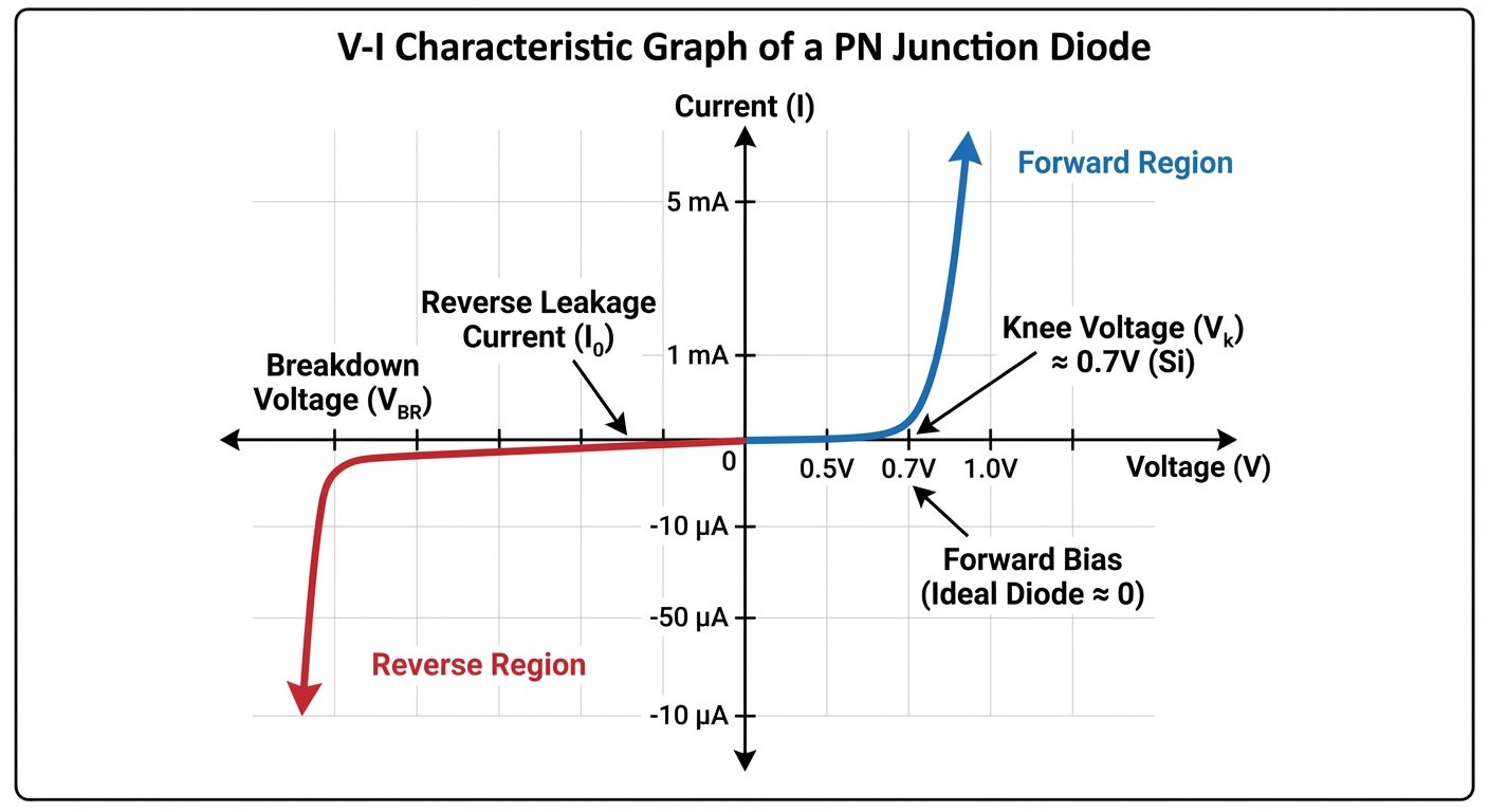
To experimentally analyze the Voltage-Current (V-I) characteristics of a silicon PN junction diode in both Forward Bias and Reverse Bias conditions. To determine the Cut-in (Knee) Voltage and calculate the Static and Dynamic resistance.
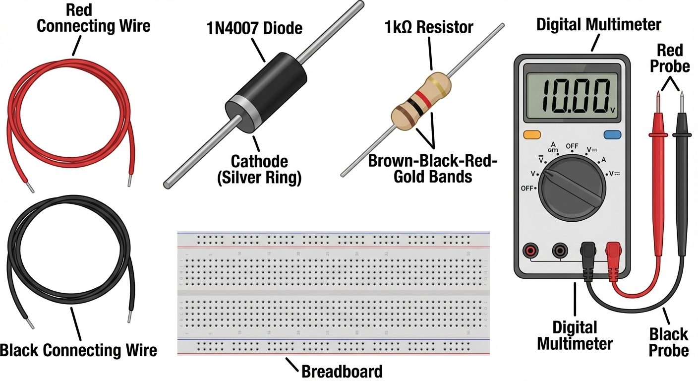
2. Apparatus/Components Required
| S.No | Component/Equipment | Specification/Value | Quantity |
|---|---|---|---|
| 1 | PN Junction Diode | 1N4007 or 1N4001 | 1 |
| 2 | Resistor (Current Limiting) | or , | 1 |
| 3 | Regulated Power Supply (RPS) | 0-30V DC, Variable | 1 |
| 4 | DC Voltmeter (or DMM) | 0-2V / 0-20V Range | 1 |
| 5 | DC Ammeter (or DMM) | 0-200mA (for FB), 0-200A (for RB) | 1 |
| 6 | Breadboard | Standard | 1 |
| 7 | Connecting Wires | Single strand | As required |
3. Theory
A PN junction diode is a two-terminal semiconductor device that allows current to flow primarily in one direction.
- Forward Bias: When the P-type region (Anode) is connected to the positive terminal and N-type (Cathode) to the negative terminal of the supply. The potential barrier is reduced. Current flows freely once the external voltage exceeds the Barrier Potential () or Cut-in Voltage (approx. 0.7V for Silicon and 0.3V for Germanium).
- Reverse Bias: When the P-type is connected to negative and N-type to positive. The depletion region widens, preventing majority carrier flow. Only a very small Reverse Saturation Current () flows due to minority carriers until the breakdown voltage is reached.
The relationship is governed by the Shockley Diode Equation:

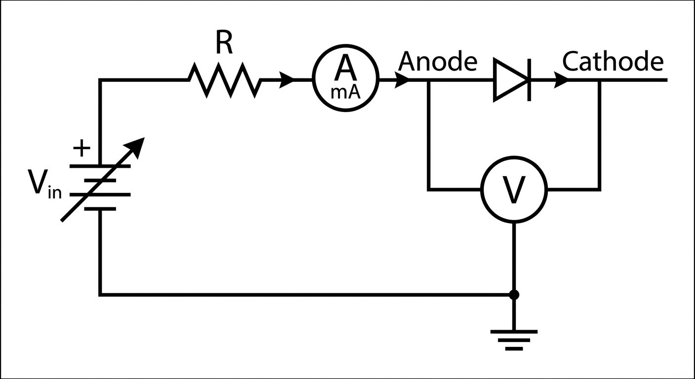
4. Circuit Diagram / Setup
A. Forward Bias Setup
In this configuration, the Anode is positive with respect to the Cathode.
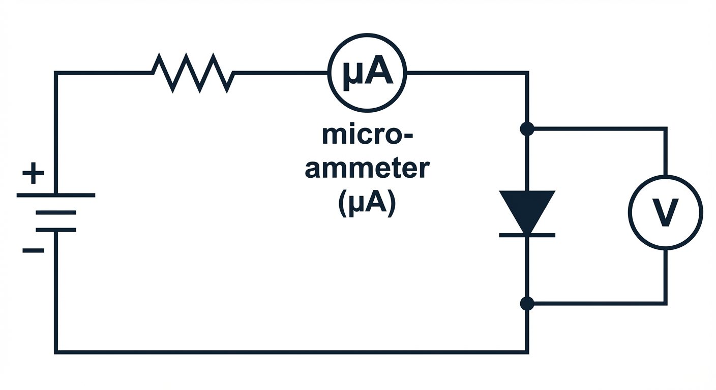
B. Reverse Bias Setup
In this configuration, the Cathode is positive with respect to the Anode. Note that the ammeter must be set to micro-amperes ().
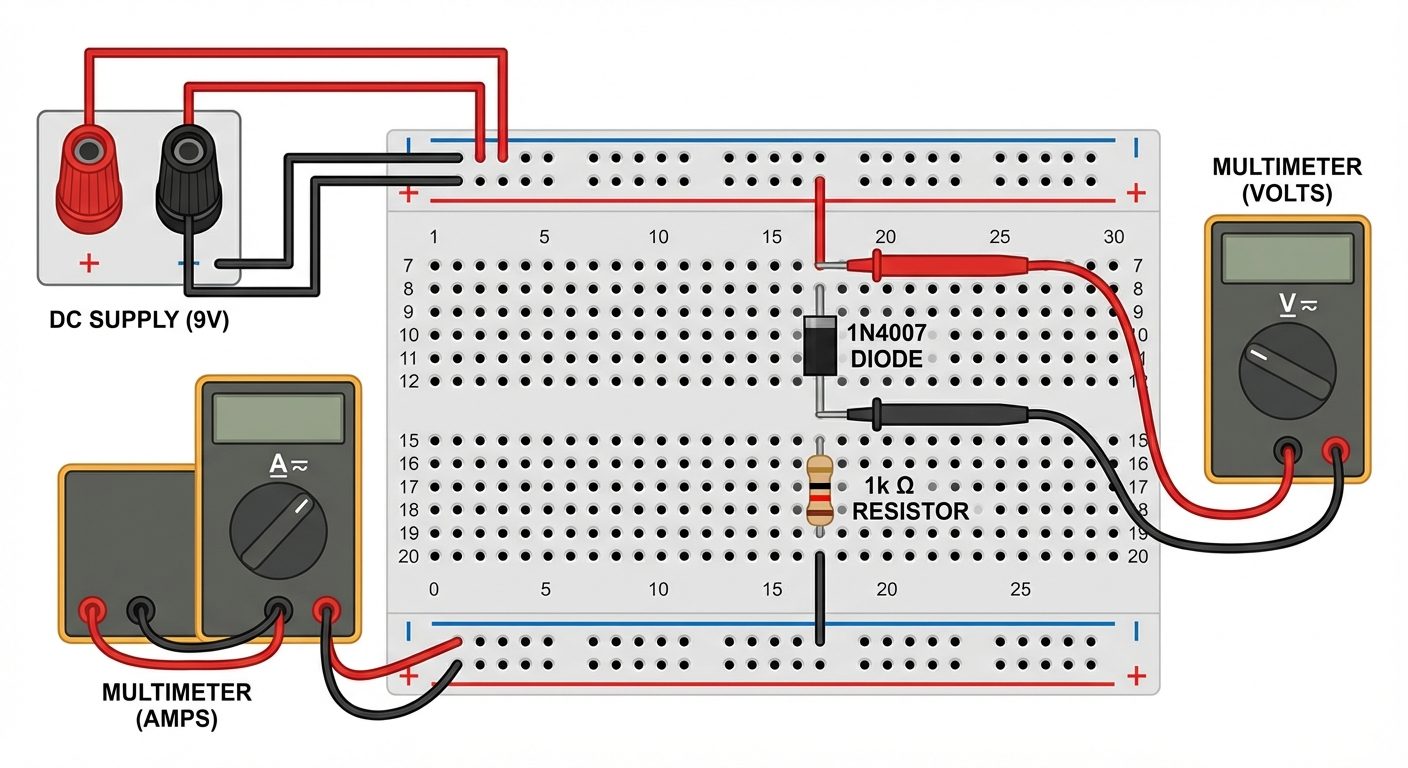
C. Physical Connection Layout (Breadboard)
5. Procedure
Part A: Forward Bias Characteristics
- Connect the circuit as shown in the Forward Bias Circuit Diagram.
- Set the DC Power Supply voltage to 0V initially.
- Gradually increase the supply voltage in small steps (e.g., 0.1V steps up to 0.8V, then 0.5V steps).
- For every step, record the Voltage across the diode () using the voltmeter and the Current through the diode () using the milli-ammeter.
- Notice that current remains negligible until voltage reaches approx. 0.6V - 0.7V (Knee Voltage).
- Beyond 0.7V, current increases rapidly. Do not exceed the maximum current rating of the diode.
Part B: Reverse Bias Characteristics
- Turn off the power supply and rearrange the circuit as shown in the Reverse Bias Circuit Diagram (reverse the diode polarity).
- Change the ammeter setting to Micro-ampere () range (or use a more sensitive meter).
- Increase the supply voltage in larger steps (e.g., 2V, 4V, 6V... up to 20V).
- Record the Voltage across the diode () and the leakage Current ().
- Note that the current is very small and nearly constant.
6. Observations and Readings
Diode Type: Silicon (1N4007)
Room Temperature:
Table 1: Forward Bias Readings
| S.No | Source Voltage () | Diode Voltage () [Volts] | Diode Current () [mA] |
|---|---|---|---|
| 1 | 0.0 | 0.0 | 0.0 |
| 2 | 0.2 | 0.2 | 0.0 |
| 3 | 0.4 | 0.4 | 0.0 |
| 4 | 0.5 | 0.5 | 0.1 |
| 5 | 0.6 | 0.6 | 0.8 |
| 6 | 0.65 | 0.65 | 2.5 |
| 7 | 0.7 | 0.7 | 8.0 |
| 8 | 0.75 | 0.72 | 15.0 |
| 9 | 1.0 | 0.74 | 30.0 |
| 10 | 2.0 | 0.76 | 60.0 |
Table 2: Reverse Bias Readings
| S.No | Source Voltage () | Diode Voltage () [Volts] | Diode Current () [] |
|---|---|---|---|
| 1 | 0 | 0 | 0 |
| 2 | 2 | 2.0 | 0.01 |
| 3 | 5 | 5.0 | 0.02 |
| 4 | 10 | 10.0 | 0.02 |
| 5 | 15 | 15.0 | 0.03 |
7. Graph and Calculations
Plot a graph with Voltage () on the X-axis and Current () on the Y-axis.
- Quadrant I: Forward Bias (V in Volts, I in mA).
- Quadrant III: Reverse Bias (V in Volts, I in ). Note: Scales for I will differ significantly.
Calculations:
From the Forward Bias graph, select an operating point (Q-point) on the linear rising portion.
1. Static DC Resistance ():
Example: At , :
2. Dynamic AC Resistance ():
Example: Between and :
8. Result
- The V-I characteristics of the PN junction diode were plotted.
- The Cut-in (Knee) voltage for the Silicon diode is found to be approximately ___ V (Expected ~0.7V).
- The diode conducts current in forward bias only after overcoming the barrier potential and blocks current in reverse bias (acting as an open switch).
9. Viva Questions
- What is the "Knee Voltage"?
- Answer: It is the forward voltage at which the current through the junction starts to increase rapidly. For Silicon, it is ~0.7V; for Germanium, ~0.3V.
- Why do we use a resistor in series with the diode?
- Answer: To limit the current flowing through the diode. Without it, once the voltage exceeds 0.7V, current would rise infinitely, burning out the diode.
- What is PIV?
- Answer: Peak Inverse Voltage. It is the maximum voltage a diode can withstand in reverse bias without breaking down.
- Why is the reverse current in micro-amperes?
- Answer: Reverse current is caused by minority charge carriers (thermally generated), which are very few in number compared to majority carriers.
- How do you identify the terminals of a diode physically?
- Answer: The terminal near the silver/grey band on the black body is the Cathode (-), and the other end is the Anode (+).