Unit 1 - Notes
Unit 1: Fundamentals of Electrical Laws, Semiconductor Devices and its Applications
1. Fundamentals of Electrical Laws
1.1 Ohm’s Law
Ohm's Law states that the current () flowing through a conductor between two points is directly proportional to the voltage () across the two points, provided the physical conditions (like temperature) remain constant.
- Formula:
- = Voltage in Volts (V)
- = Current in Amperes (A)
- = Resistance in Ohms ()
- Limitations: Not applicable to non-linear devices (diodes, transistors), non-metallic conductors, or varying temperatures.
1.2 Kirchhoff’s Laws
These laws govern the conservation of charge and energy in electrical circuits.
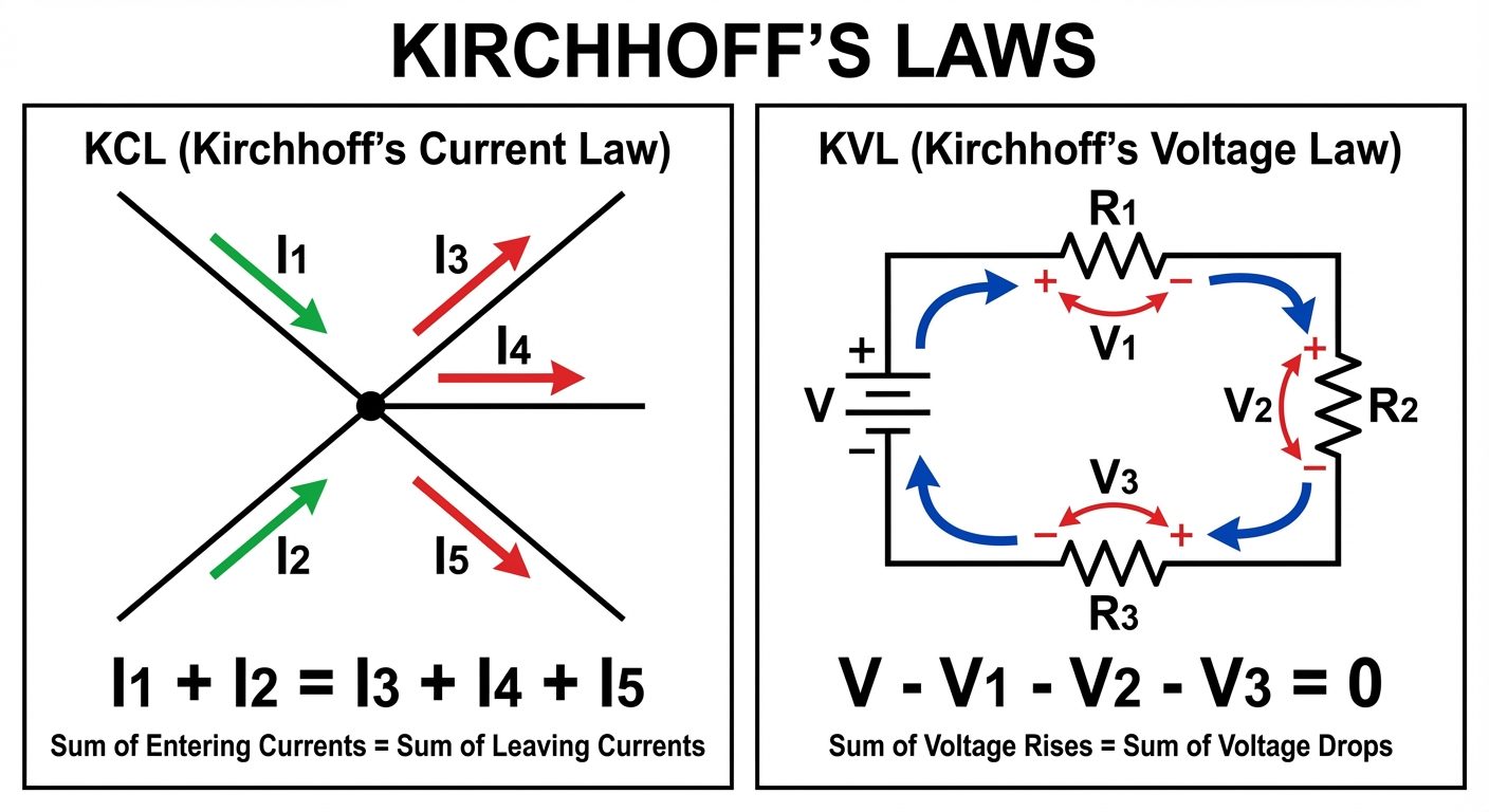
A. Kirchhoff’s Current Law (KCL)
- Statement: The algebraic sum of currents entering a node (junction) is equal to the sum of currents leaving the node. Alternatively, the algebraic sum of currents at a node is zero.
- Principle: Conservation of Charge.
- Formula:
B. Kirchhoff’s Voltage Law (KVL)
- Statement: In any closed loop (mesh), the algebraic sum of all voltage drops (across resistors) and EMFs (voltage sources) is equal to zero.
- Principle: Conservation of Energy.
- Formula: or
1.3 Circuit Division Rules
Voltage Division Rule (Series Circuits)
Used to find the voltage across a specific resistor in a series circuit.
- The voltage drops across resistors are proportional to their resistance values.
- Formula:
Current Division Rule (Parallel Circuits)
Used to find the current flowing through a specific branch in a parallel circuit.
- Current divides inversely proportional to resistance.
- Formula (for two resistors ):
- Current through :
- Current through :
2. Basics of Semiconductors
Semiconductors are materials (typically Silicon or Germanium) whose conductivity lies between conductors and insulators.
2.1 Intrinsic Semiconductors
- Definition: Semiconductors in their purest form without any impurities.
- Carrier Concentration: The number of free electrons () equals the number of holes (). .
- Conductivity: Low at room temperature; increases with temperature.
2.2 Extrinsic Semiconductors
Formed by adding impurities (doping) to intrinsic semiconductors to increase conductivity.
| Feature | N-Type Semiconductor | P-Type Semiconductor |
|---|---|---|
| Dopant | Pentavalent (Group V) e.g., Phosphorus, Arsenic | Trivalent (Group III) e.g., Boron, Indium |
| Majority Carriers | Electrons (Negative charge) | Holes (Positive charge) |
| Minority Carriers | Holes | Electrons |
| Net Charge | Neutral | Neutral |
3. PN Junction Diode
3.1 Construction and Formation
Formed by metallurgically joining a P-type semiconductor and an N-type semiconductor.
- Depletion Region: Near the junction, electrons from the N-side diffuse to the P-side and recombine with holes. This creates a region devoid of free carriers containing only immobile ions.
- Barrier Potential: An electric field is created across the depletion region ( for Silicon, for Germanium).
3.2 Biasing and Working
- Forward Bias:
- P-terminal connected to Positive (+), N-terminal to Negative (-).
- Depletion width decreases.
- Current flows easily once barrier potential is overcome.
- Reverse Bias:
- P-terminal connected to Negative (-), N-terminal to Positive (+).
- Depletion width increases.
- Ideally no current flows (practically, a tiny leakage current exists).
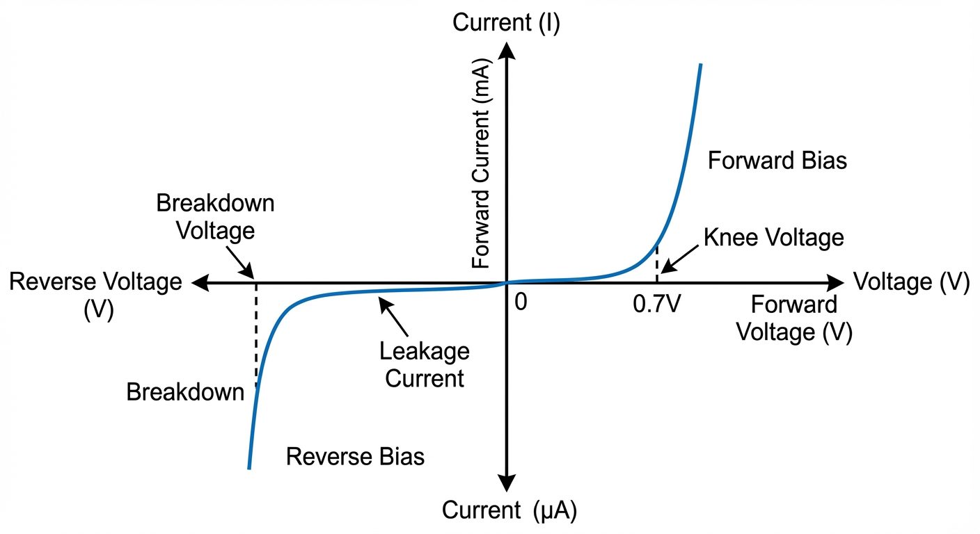
3.3 V-I Characteristics
The Voltage-Current characteristic curve describes the diode's behavior.
- Forward Region: Current rises exponentially after the Knee Voltage (Cut-in voltage).
- Reverse Region: Minimal current (Reverse Saturation Current) until Breakdown Voltage is reached, where current spikes dangerously.
3.4 Applications
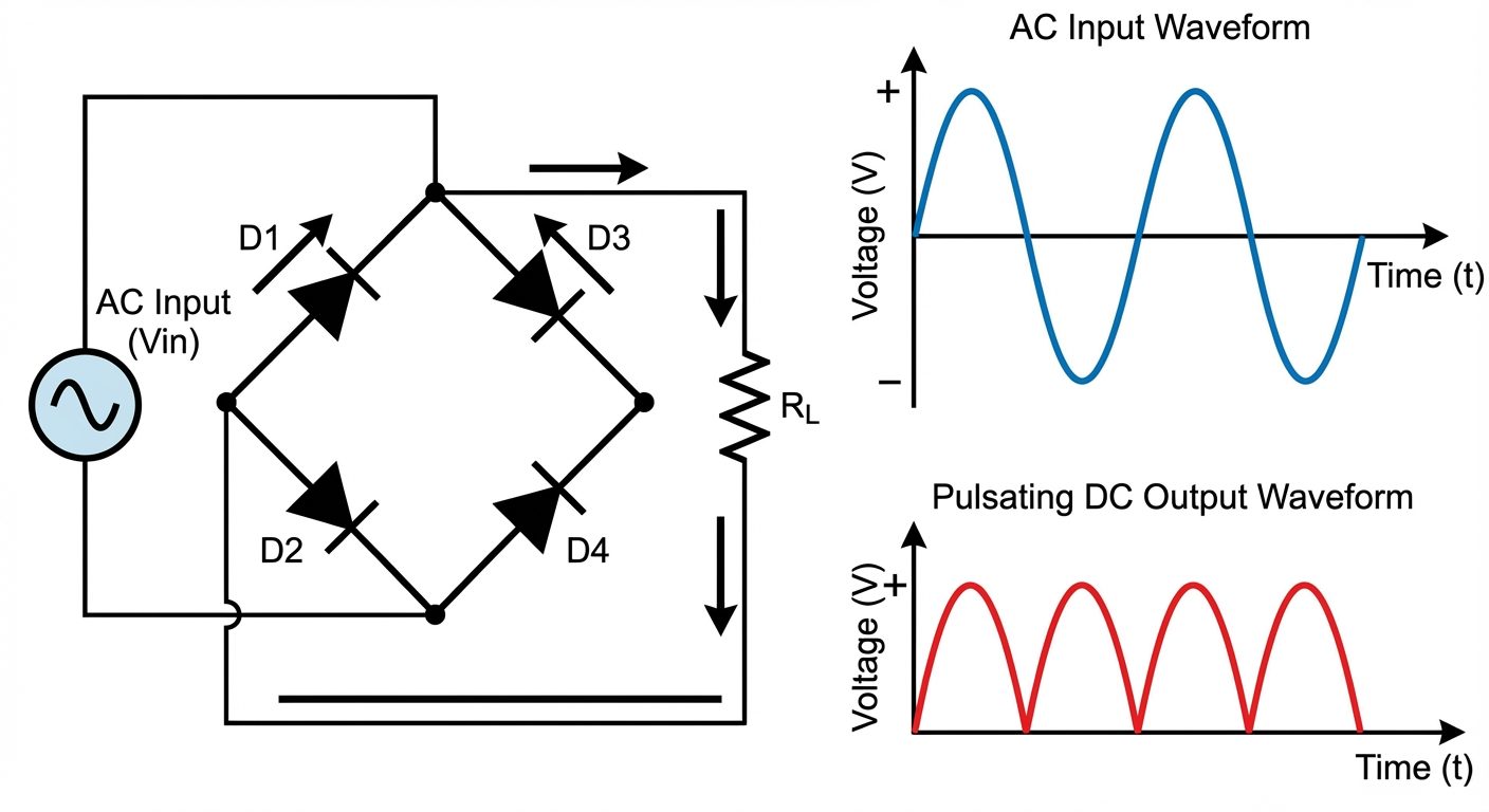
A. Rectifiers
A rectifier converts Alternating Current (AC) into pulsating Direct Current (DC).
- Half-Wave Rectifier: Uses 1 diode. Conducts only during the positive half-cycle of input AC. Efficiency .
- Full-Wave Bridge Rectifier: Uses 4 diodes in a bridge topology. Conducts during both positive and negative half-cycles. Efficiency .
B. Diode as a Switch
- ON State: When Forward Biased, resistance is very low (), acting as a closed switch.
- OFF State: When Reverse Biased, resistance is very high (), acting as an open switch.
4. Bipolar Junction Transistor (BJT)
A BJT is a three-terminal, current-controlled device used for amplification and switching.
4.1 Construction
- Terminals:
- Emitter (E): Heavily doped, emits carriers.
- Base (B): Lightly doped, very thin, passes carriers from E to C.
- Collector (C): Moderately doped, large physical size, collects carriers.
- Junctions: Emitter-Base Junction () and Collector-Base Junction ().
4.2 Types
- NPN: P-type base sandwiched between two N-regions. (Current flows C to E).
- PNP: N-type base sandwiched between two P-regions. (Current flows E to C).
4.3 Modes of Operation
| Mode | Emitter-Base Junction () | Collector-Base Junction () | Application |
|---|---|---|---|
| Active | Forward Biased | Reverse Biased | Amplifier |
| Saturation | Forward Biased | Forward Biased | Switch (ON) |
| Cut-off | Reverse Biased | Reverse Biased | Switch (OFF) |
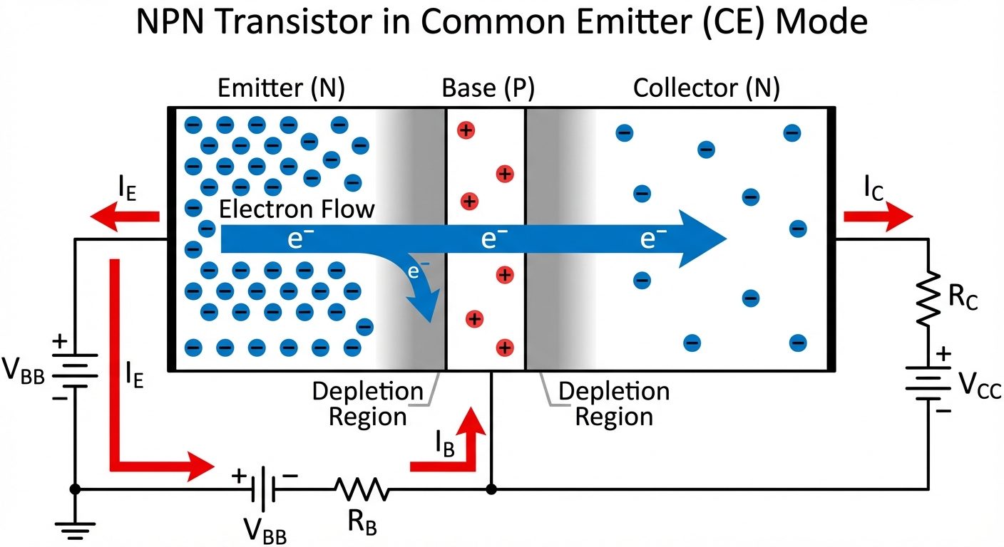
4.4 Working of NPN Transistor (CE Configuration)
In the Common Emitter (CE) configuration, the Emitter is common to both input and output.
- Biasing: Base-Emitter is Forward Biased (), Collector-Base is Reverse Biased ().
- Process:
- Electrons from the N-type Emitter cross into the P-type Base.
- Since the Base is thin and lightly doped, only a few electrons () recombine with holes (constituting Base Current ).
- The remaining electrons () are attracted by the high positive potential of the Collector, crossing (constituting Collector Current ).
- Current Equation:
4.5 CE Configuration Characteristics
Input Characteristics
- Plot of Input Current () vs Input Voltage () at constant Output Voltage ().
- Resembles the forward characteristics of a diode. Current increases after .
Output Characteristics
- Plot of Output Current () vs Output Voltage () at constant Input Current ().
- Three Regions:
- Cut-off: Both junctions reverse biased; .
- Saturation: Both junctions forward biased; increases rapidly with .
- Active: forward, reverse; is constant regardless of (amplification region).